Invited Lecture
THERMAL STABILITY AND MICROSTRUCTURAL EVOLUTION OF NITRIDE-BASED METAL/SEMICONDUCTOR SUPERLATTICES
A detailed analysis on the quality and microstructure of various metal/semiconductor superlattices employing HR(S)/TEM (high-resolution (scanning)/transmission electron microscopy) imaging and energy dispersive x-ray spectroscopy (EDX) mapping on as-deposited and annealed samples is presented.
Epitaxial metal/semiconductor superlattices are known to be promising candidates for compounds in electronic, photonic, and plasmonic devices, but are also of interest for applications as hard coatings, and in thermoelectric materials [1]. The crystalline quality of the superlattices, in terms of their defect density, phase purity, interface roughness, and stoichiometry of the individual layers, plays a crucial role with respect to the physical properties and thus the applicability of such superlattice stacks. It was recently shown that metal/semiconductor superlattices based on (Al,Sc)N as the semiconductor component can be grown epitaxially with low-defect densities by magnetron sputtering on [001]MgO substrates [2].
Phase formation and thermal stability studies of as-deposited and long-time annealed cubic TiN/(Al,Sc)N superlattices employing a combination of HR(S)/TEM and EDX mapping revealed intermixing of the TiN and (Al,Sc)N layers by interdiffusion of the metal atoms with increased annealing time [3].
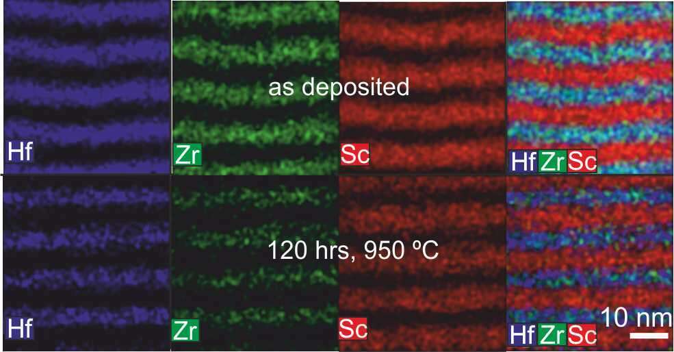
Improved (Ti,W)N/(Al,Sc)N [4] and (Hf,Zr)N/ScN [5] superlattices were grown by magnetron sputtering and analyzed with various TEM methods, and their microstructural evolution as well as thermal stability becomes presented here. Figure 1 demonstrates thermal stability of ZrxHf1-xN/ScN by comparing an as-deposited with a 120 hrs annealed superlattice stack via EDX mapping.
All experiments were conducted at Linköping’s image- and probe-corrected and monochromated FEI Titan3 60-300 microscope equipped with a Gatan Quantum ERS GIF, high-brightness XFEG source, and Super-X EDX detector, operated at 300 kV [6].
References:
- T. D. Sands, C.J. Palmstrøm, J.P. Harbison, V.G. Keramidas, N. Tabatabaie, T.L. Cheeks, Y. Silberberg, Stable and epitaxial Metal/III-V semiconductor heterostructures, Mater. Sci. Rep. 5: 98–170, 1990.
- B. Saha, S. Saber, G.V. Naik, A. Boltasseva, E.A. Stach, E.P. Kvam, T.D. Sands, Development of epitaxial AlxSc1-xN for artificially structured metal/semiconductor superlattice metamaterials, Phys. Status Solidi B, 252, 2, 251-259, 2015.
- J. L. Schroeder, B. Saha, M. Garbrecht, N. Schell, T. D. Sands, and J. Birch, Thermal stability of epitaxial cubic-TiN/(Al,Sc)N metal/semiconductor superlattices, J. of Mater. Sci., 50: 3200-3206, (2015).
- B. Saha, Y. R. Koh, J. Comparan, S. Sadasivam, J. L. Schroeder, M. Garbrecht, J. Birch, D. Cahill, T. Fisher, A. Shakouri, and T. D. Sands, Cross-plane thermal conductivity of (Ti,W)N/(Al,Sc)N metal/semiconductor superlattices, Phys. Rev. B, 93, 045311, 2016.
- M. Garbrecht, J. L. Schroeder,L. Hultman, J. Birch, T. D. Sands, and B. Saha, Microstructural evolution and thermal stability of ZrxHf1-xN/ScN (x = 0, 0.5, 1) metal/semiconductor superlattices. submitted, 2016.
- 6. We acknowledge the Knut and Alice Wallenberg (KAW) Foundation for the Electron Microscope Laboratory in Linköping.
|