Spherical aberration correction has become inevitable in materials science for atomic-resolution imaging of conventional objects by transmission electron microscopy at medium accelerating voltages (80-300kV). However, low-Z objects and radiation-sensitive low-dimensional objects require lower accelerating voltages because the threshold for knock-on damage is below 80kV for these materials. Unfortunately, the resolution of spherical aberration-corrected transmission electron microscopy at an accelerating voltage less than 80 kV with a standard Schottky type or field-emission electron source is strongly limited by the chromatic aberration of the objective lens.
Here we report on our approach to achieve atomic resolution at voltages in the range between 20-80kV in transmission electron microscopy [1, 2]. We employ for our investigations the newly-developed aberration corrector that corrects for both, spherical and chromatic aberration of the objective lens. First experimental results of low-dimensional objects will be presented.
The excellent performance of the SALVE (Sub-Angstrom Low-Voltage Electron microscopy) microscope enables atomic-resolution imaging and high-resolution energy-filtered (EF)-TEM with large energy windows even at 20kV accelerating voltage. Moreover, we discuss sample preparation approaches [3,4] and show first results on low-dimensional objects. Using, as an example, high-resolution imaging of graphene and MoS2, we compare quantitatively the contrast between experiment and calculation. Obviously, no damping of the contrast transfer function by chromatic aberration has to be considered in the image calculation routine, although image spread due to thermal magnetic field noise [5] has been taken into account as a new source of contrast transfer damping. The envelope in calculations results from image-spread and residual defocus [6, 7]. The calculations are performed in dependence of the dose [7]. Figure 1 shows an experimental HRTEM image of single-layer graphene at 30kV. The usable aperture of about 65mrad shows that an information limit of 107 pm has been achieved. The comparison of the line profiles through the calculated and experimental images demonstrates that a good match has been obtained. [8]
References
[1] U Kaiser et al, Ultramicroscopy 111 (2011), p. 1239.
[2] www.salve-projcet.de
[3] G Algara-Siller et al. Appl. Phys. Lett. 104 (2014), p. 153115.
[4] G Algara-Siller et al. Appl. Phys. Lett. 103 (2013), p. 20310.
[5] S. Uhlemann et al., Physical Review Letters 111(4) (2013), p.046101.
[6] M. Haider, P. Hartel, H. Müller et al, Microsc. Microanal. 16(2010), p 393-408.
[7] Z. Lee, H. Rose, O. Lehtinen et al, Ultramicroscopy 145(2014), p 3-12.
[8] The authors greatly acknowledge funding from the German Research Foundation (DFG) and the Ministry of Science, Research and the Arts (MWK) of the federal state Baden-Württemberg, Germany in the frame of the SALVE project.
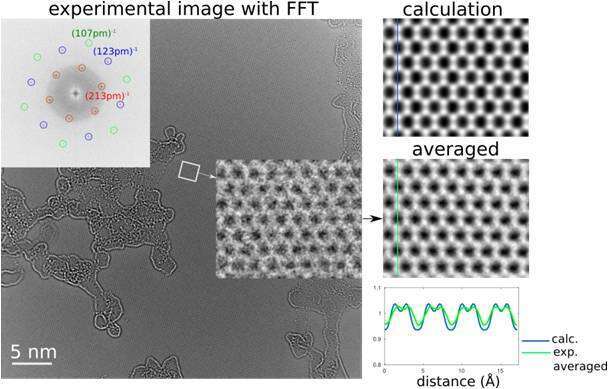
Fig.1 (left): 30 kV CC/CS-corrected HRTEM raw image of graphene with inserts: top left: diffractogram of the whole area, middle right: magnified image of the white rectangular, (right column): Comparison between calculated (top) and averaged experimental (middle) images, the corresponding lines are shown as profiles below.