
Short wavelength infrared InAs/InSb/AlSb Type-II superlattice photodetector
2Solid State Physics Department, SCD-SemiConductor Devices
A photdetector based on InAs/InSb/AlSb type-II superlattice (T2SL) with thicknesses of 15, 1 and 4 monolayers (MLs) respectively was fabricated and characterized. Hoang et al. (2012 APL) already showed that a ML of GaSb sandwiched between AlSb and InAs (T2SL), confines the holes wave function and increase λcutoff toward the 2-3 µm region. In this work, using a one ML of InSb sandwiched between 4 ML of AlSb and 15 ML of InAs, a λcutoff of 3.3 µm was measured (Fig .1). A complete simulation study will be published elsewhere.
The InAs/InSb/AlSb T2SL was grown using molecular beam epitaxy (MBE) system. The superlattice period of Λ~6 nm was extracted using Λ=λCu-Ka/2[sin(θ1)-sin(θ2)], where λCu-Ka=0.15 nm is the X-ray wavelength and 2θ1,2 are shown in the X-ray diffraction results, Fig. 2.
The device layers structure and process flow described in Fig. 3. The mesas were etched using H2O:H3PO4:H2O2 and a standard liftoff process of Ti/Au contact was performed by lithography. Finally the samples were mounted and bonded to a jig and loaded into a cryostat for characterization.
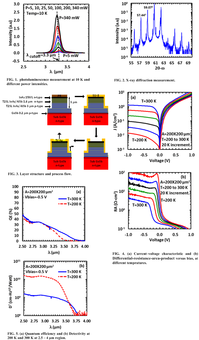
For the 200 µm mesa device, with -0.5 V bias, the dark current at 300 and 200 K was 1.1 and 8.5X10⁻³ A/cm2 respectively as shown in the current voltage characteristic, Fig. 4. The quantum efficiency at λ=2.75 µm for both 300 K and 200 K was 34 % (Fig. 5a) and the detectivity was above 109 Jones for 300 K and above 1010 Jones for 200 K between 2.5-3 µm wavelength (Fig. 5b).
Powered by Eventact EMS