
Type II Superlattice- Based Detectors for Short-Wave Infra-Red Detection (1.7-2.5µm)
2Applied Physics Department, Hebrew University
3Semi-Conductor Devices, SCD
Short-Wave Infra-Red (SWIR) photodetectors which operate beyond the response cutoff of InGaAs- based detectors (1.7-2.5µm) are required for both defense and civil applications. Existing SWIR high- responsivity detectors are based mostly on two technologies, unmatched InGaAs/InP layers, and MCT layers, but both are inadequate for realization of low price Focal Plane Arrays (FPAs).
The use of Type II Super-Lattices (T2SL) was recently proposed as a candidate for near- room temperature SWIR detection. The layers structure is based on alternating Nano-layers, serving as adjacent quantum wells for electrons and holes, with adjustable ground states alignment effectively allowing band gap engineering. The design of the layers enables tuning of the artificial detection cutoff, thereby reducing temperature- related noise.
The work presented here focuses on a T2SL based on alternating Nano-layers of InGaAs and GaAsSb, grown by MBE, lattice- matched to an InP substrate. Mesa- and selective diffusion- based PIN photodiode devices were designed, simulated, fabricated and characterized.
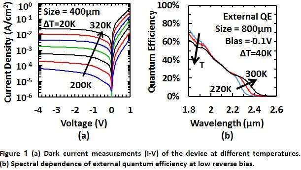
At room temperature, Mesa- based devices exhibit cutoff wavelength of 2.4µm with dark currents of 1.3mA/cm2, implying SWIR detectivity above 1010 Jones. Dark currents were lowered below 1mA/cm2 by utilizing a selective diffusion process significantly improving peripheral current contribution. The results show promising high-quantum efficiency SWIR detection, while exhibiting relatively low dark currents.
Powered by Eventact EMS