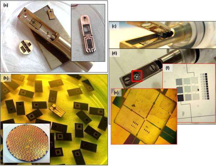
We design and fabricate an electrical biasing TEM holder and samples, for electron-optical experiments.
There are many variants of commercial TEM sample holders today, for in-situ experiments. Some include heating or cryo capabilities, liquid cell, nanoindentation, and electrical biasing. These, however, are meant for materials or biological research. We are in the process of fabricating a specialized electrical biasing holder, with the aim of modulating the electron beam in-situ. Such a modulated beam could be used as a tool for specialized research in electron optics or fabrication of nano elements. We begin with an old heating holder, which has the benefit of being hollow for putting conductive wiring through. The tip is replaced with a CAD-planned new tip, fabricated in a university’s mechanical workshop. I then use a femtosecond laser micromachining machine to carve a rectangular depression into the tip, which would accommodate a replaceable chip (a). At the same time, a vacuum-friendly printed circuit board is also laser-milled to produce electrical copper contacts leading to the chip (a-inset). To fabricate the chips, I use a standard photolithography process, starting with a commercial silicon wafer coated with 200nm of silicon nitride. The four contacts are gold-evaporated, whereafter the wafer is diced and the silicon is chemically etched to form a thin silicon-nitride membrane (b). When put together, the device is complete, see (c) and (d). With many chips now available, I use electron beam lithography to fabricate small conductive structures on the membrane itself, e.g. (e) and (f). In (f), for example, the membrane is coated with aluminum, and the visibly marked lines are where the aluminum has been etched; this results in four areas, each controlled with a different electrical contact. The snake-like curve is intended to be used as a dynamic Bragg grating for electrons, giving the ability to control diffraction efficiency with variable voltage.


