Circuit editing and wire bonding modifications are occasionally required during packaging qualification and failure analysis of Integrated Circuits and Micro Electronic Components.
In this work we report on a unique method of utilizing Dual Beam Focused Ion Beam (FIB) for quick and reliable modification of devices assembled in plastic packages. Two examples of cutting, manipulating and repairing gold wire bonds is presented.
Case 1:
In order to expose the wire-bonding of the Silicon die, for debugging purposes, of a failing Plastic Ball Grid Array (PBGA) packaged unit, its epoxy cover is normally etched away using chemical acids.
During the decapsulation process of a failing unit, one of the gold wire bonds (A in fig.1) has unintentionally been detached from its bonding pad, thus affecting the functionality of the device. Since reconnecting the broken wire bond using a conventional wire bonding machine could damage this device, we performed the bonding process using FIB:
The edge of the FIB manipulator’s probe needle was used as a “patch” to minimize the bending of the wire for its reconnection (B in fig.1). Then the wire bond was slightly bent towards the edge of the patch using the FIB manipulator. The edge of the wire was finally connected to the top of the patch by forming a conductive connection, using the Platinum gas injection source (GIS) (fig.2). Electrical testing confirmed that the device regained its basic functionality and ready for debugging!
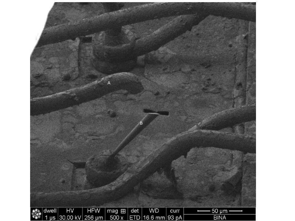
Figure 1: Disconnected wire (A) and prober edge attached to pad for extension (B).
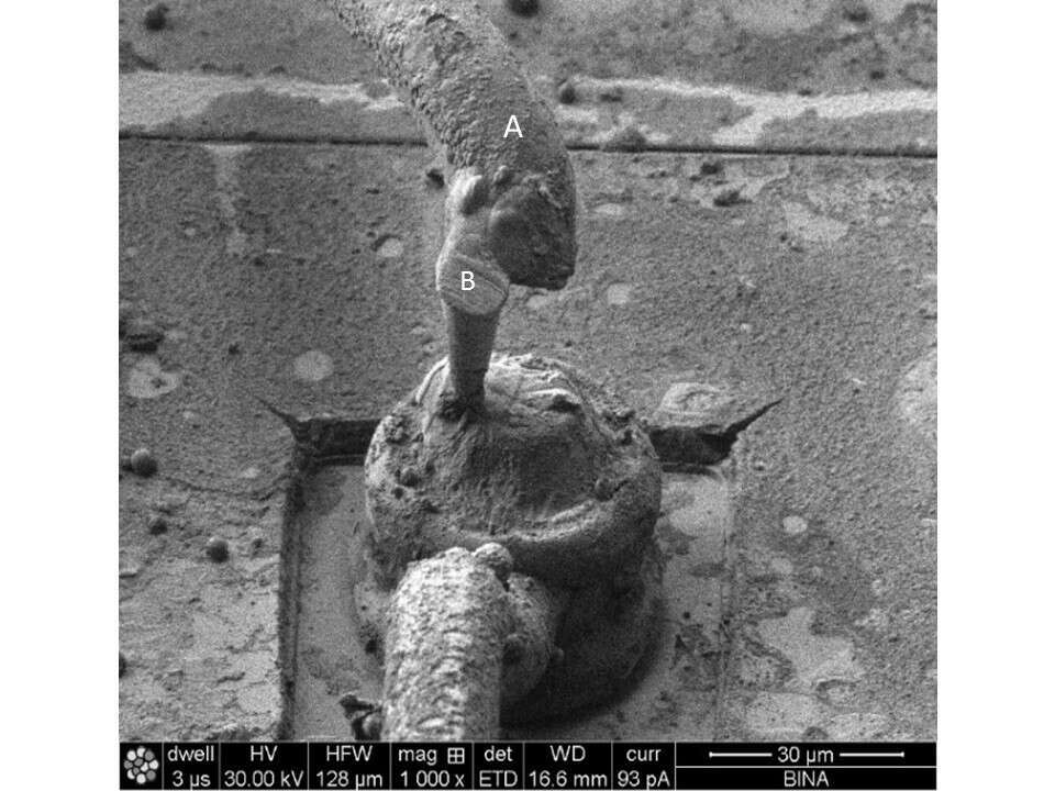
Figure 2: Reconnected wire bond.
Case 2:
Two adjacent wirebonds were found to be incorrectly connected to their pads and required to be switched with each other. Since the above mentioned FIB process is much more reliable and faster than the conventional wirebonding process it was utilized for this modification too. Following decapsulation, the two wire bonds were first cut in a predefined location found to be suitable for the editing, using FIB milling. The wire bonds were then manipulated to the desired location on the Polyimide coated surface of the die (fig.3). Two Platinum micro lines were then deposited on the die surface, establishing electrical connection between each wire and its correct pad (fig.4).
Following the FIB edit the device was tested and the bug found to be fixed by the FIB edit!
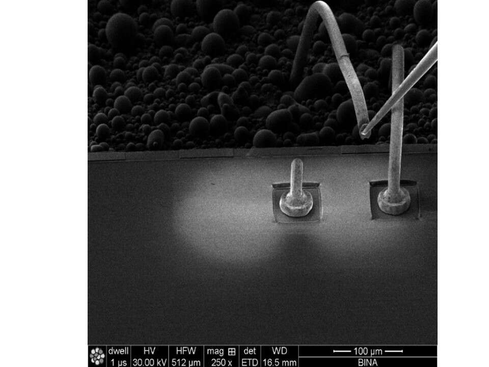
Figure 3: Cutting and manipulating the wire bond.
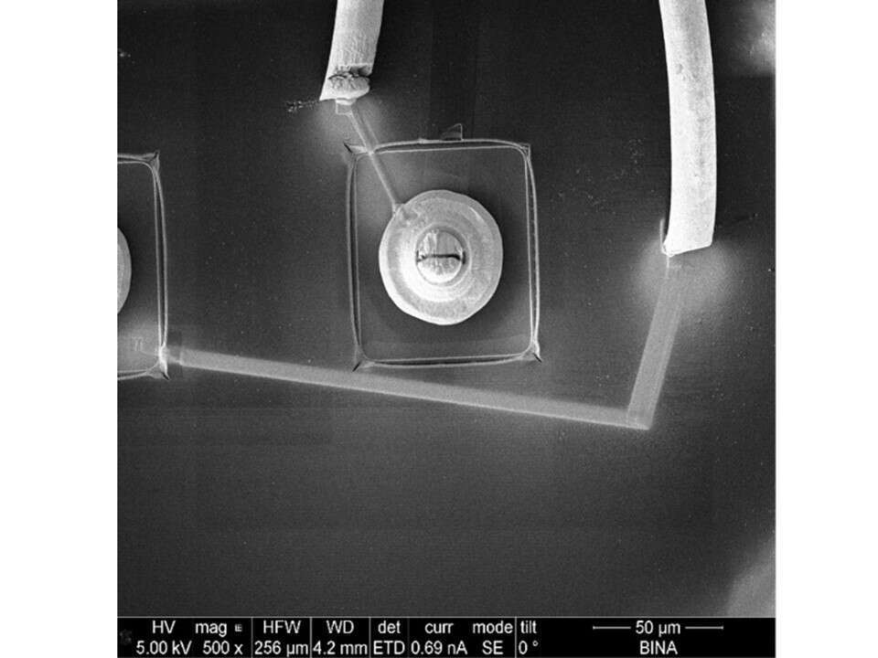
Figure 4: Reconnecting the wire bonds to the correct pads.