Here we demonstrate a nonlinear multi-layer metamaterial hologram. By Using e-beam lithography we fabricate polarization-sensitive nonlinear hologram, where the phase information of an object is encoded in computer generated plasmonic nanoantennas in the multi-layer metamaterial. By illumination the sample with a polarized infrared laser, the image of the object is reconstructed at a frequency that is the third-harmonic of the incoming beam. This is obtained by the nonlinear process of Third Harmonic Generation.
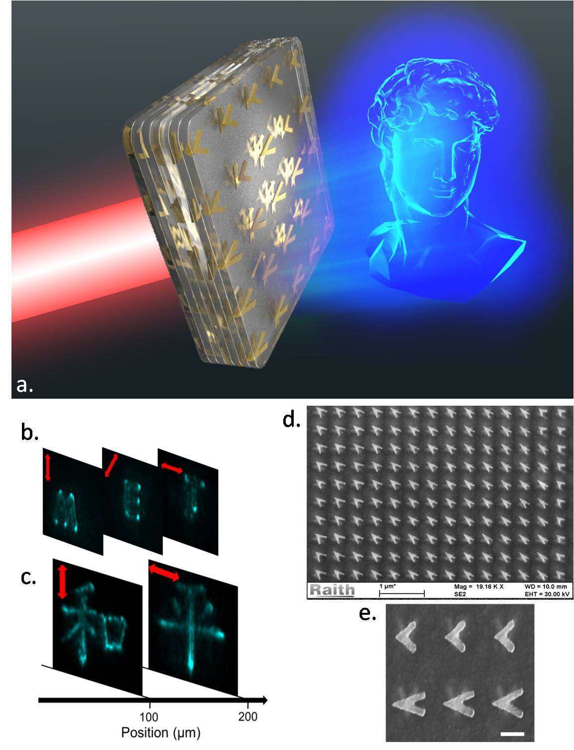
- Illustration of the concept of a multilayer nonlinear metamaterial hologram.
- Non Linear formed images of a three-layer hologram displaying the word MET (indicating the name of the Metropolitan Museum in New York). Each character is formed at a different focal distance corresponding to different light polarization (0, 45 and 90 degrees).
- Chinese characters for “Peace and harmony”. Each image of character is formed at different focal distance for different light polarization.
- SEM image of the top layer of Multilayer device.
- Higher magnification of (d). Layers underneath can be observed as well. Scale bar is 200nm.
Fabrication process
The samples are prepared by multilayer e-beam lithography on a borosilicate glass substrate. To avoid electron charging on the substrate during SEM, 3 nm thick chromium (Cr) layer was initially deposited on the substrate by e-beam evaporation. A 180 nm silica layer was grown by Plasma Enhanced Chemical Vapor Deposition (PECVD) on top of the Cr film. Then the desired design of 30 nm thick antennas is patterned by e-beam lithography. In order to fabricate a nearly flat patterned surface of gold antennas, the silica pattern is etched via Inductively Coupled Plasma (ICP) after developing the PMMA resist. Then a 2 nm thick chromium adhesion layer and a 30 nm thick gold layer were deposited on the patterns by e-beam evaporation. The resist is then lifted off in acetone in an ultrasonic bath, leaving a gold antenna buried in the SiO2 layer. A 180 nm thick silica layer is deposited on the metallic pattern by PECVD and serves as a dielectric spacer between two adjacent active nanoantenna layers. The entire fabrication process is repeated for the additional layers.