
Surface Patterning through Local Electrodeposition of Metals using Liquid/Solid & Liquid/Liquid Interface
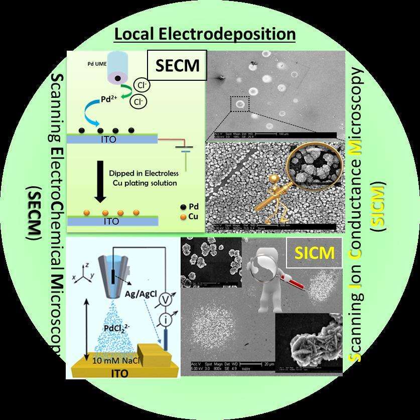
Electrochemical scanning probe methods offer an alternative approach for the deposition of micrometer or sub-micrometer structures. Scanning electrochemical microscopy (SECM) is a new approach to deposit micropatterns at the liquid/solid or liquid/liquid interface driven by electrochemistry. The feedback mode of SECM has been applied to deposit the patterned palladium (Pd) sub-micron structures from Pd microelectrode on a conducting and insulating substrates. The Pd patterns on the surface are further modified with electroless copper plating solution to obtain copper microstructure on the flexible and transparent surface. A similar approach, widely known as scanning ion conductance microscopy (SICM) has also been introduced here for the localized electrochemical deposition of Pd using a pulled micropipette as a tip. In contrast to the other scanning probe microscopy technique, SICM is still under development, especially in terms of local electrodeposition. Herein, the micropipette is filled with palladium salt and Ag/AgCl reference is inserted in the pipette as well as in the bath solution. The application of negative potential to the electrode in the micropipette causes negatively charged ions, PdCl42-, to leave the pipette. This flux can be further reduced on a bias ITO or pretreated PET substrate. The surfaces are subsequently treated with copper electroless plating formulation. SICM has huge potential over SECM in micro/nano electronics and device fabrication.

Powered by Eventact EMS