
CHARACTERIZING OF SELF-ASSEMBLED MONOLAYER BARRIERS FOR COPPER METALLIZATION
2Department of Physical Electronics, School of Electrical Engineering, Faculty of Engineering, Tel Aviv University, Tel Aviv, Israel
3Wolfson Applied Materials Research Center, Wolfson Applied Materials Research Center, Tel Aviv, Israel
Recently, we developed a fast and safe process of Silanization of Self assembled monolayer (SAM) barriers for Cu metallization for Ultra Large Scale Integration (ULSI) for Integrated Circuit (IC) applications. The SAM was deposited on Bare-Si, thermal oxide and Low-k dielectrics using a novel process using high flash point solvents (i.e. NMP, Ethelene glycol) allowing elevated deposition temperature and short deposition time; therefore, providing higher throughput process, taking few minutes compared to few hours in conventional SMA deposition methods using low flash temperature point such as ethanol, methanol, toluene etc. The method presented here was developed for monolayers based on various silane monomers compatible with CMOS process.
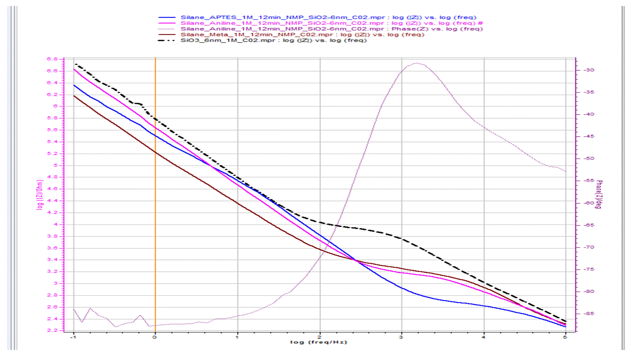
The aim of this work is to develop methods for characterizing the barrier properties and provide in line monitoring techniques that can predict barrier quality and/or barrier failures of the SAM fabricated in the new Silanization process. One approach was to examine the defect density and coverage properties of the SAM on LowK dielectric using EIS (electrochemical impedance spectroscopy) at various bias point. (Fig 1.) Another approach is to use physical methods for the characterization of Self Assembled monolayers, i.e. Variable Angle X-Ray Photoelectron Spectroscopy (Variable Angle -XPS).
Following developing of the various methods, the results are compared in order to find the most suitable method for SAM metrology and monitoring that can be employed by the Semiconductor industry.
Powered by Eventact EMS