
CONTROL OF POLYSILICON NANOWIRES CONDUCTIVITY BY ANGLE-DEPENDENT ION IMPLANTATION
2Labs, Micron Semiconductors, Kiryat Gat, Israel
3Department of Engineering, Micron Semiconductors, Kiryat Gat, Israel
Boron doped polysilicon nanowire devices were fabricated using lithography-based top-down method. The devices, implanted by boron ions at different angles (0,20,30,45º), exhibited significant dependence of electrical conductivity on incident implantation angle. Monte Carlo simulations of the dopant distribution, show that the projected range of boron implant increase with decreasing incident angle, in agreement with literature SRIM (Stopping and Range of Ion in Matter) reported data. The simulations and electrical measurements, show that geometrical shadowing reduce the device conductivity, while lower incident implantation angles increase it. This implies that Polysilicon Nanowires conductivity can be controlled by changing the implant angle, and this is beneficial for ‘top=down’ fabrication of SiNW sensors based on accumulation and depletion.
KEYWORDS: Nanowires, Top-down, polycrystalline silicon, Ion implantation, Monte Carlo simulation
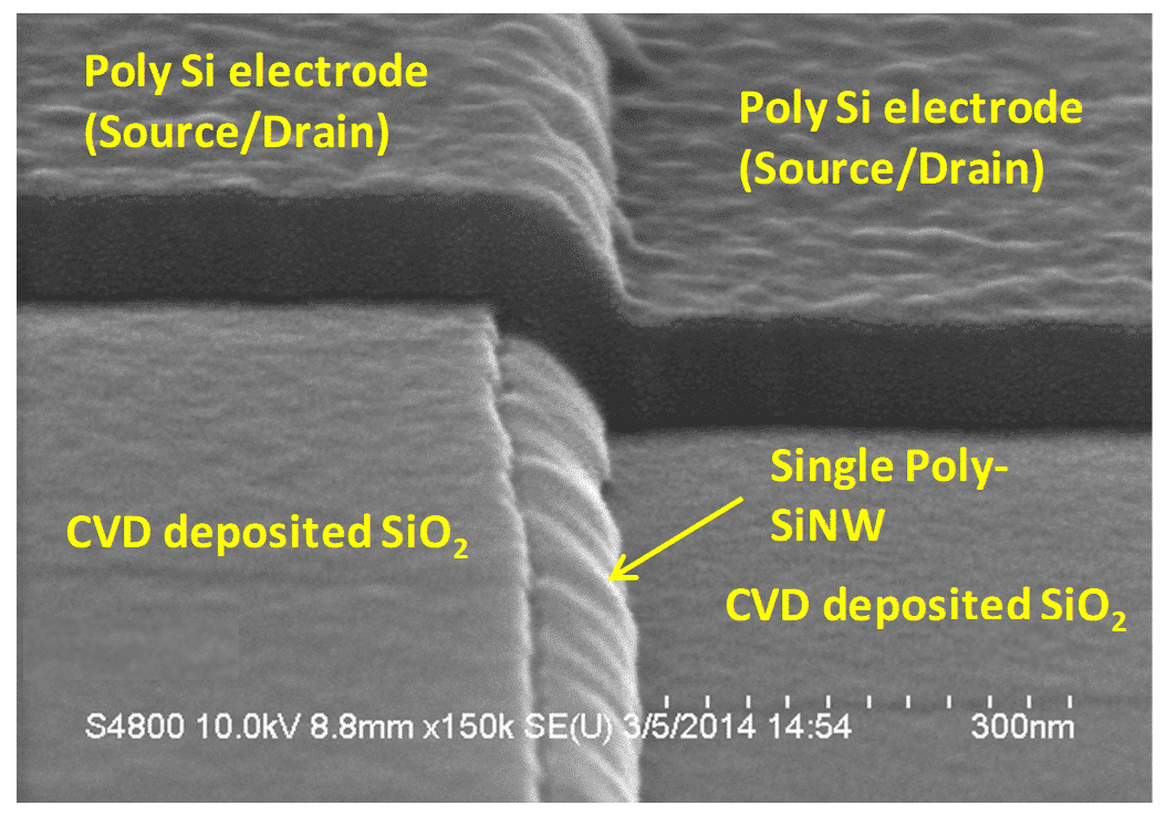
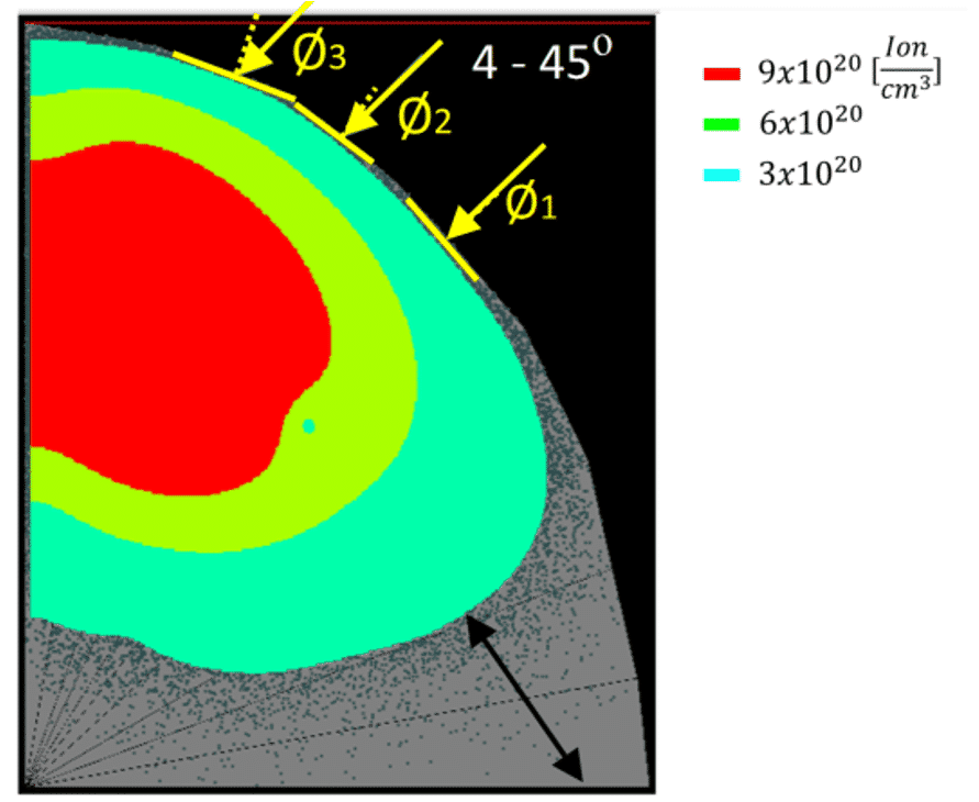
1. Close-up SEM image showing a single SiNW connected to an electrode. 2.Post anneal dopant simulation of 45º boron implanted SiNW using Monte-Carlo simulator [ions/cm3].
Powered by Eventact EMS