
Excitation Voltage Switching Circuit for G.M Detectors
2Electronic & Control Laboratories, Nuclear Research Center Negev
Introduction
In order to extend the effective count range of a Geiger tube, there comes the Time To Count method [1]. In this method, after a Geiger discharge, the high Voltage applied to the tube is lowered to a level where charge multiplication could not occur. The voltage is kept low for an amount of time that is enough for the collection of the positive ions (Typically 1-2 milliseconds). The high voltage is then switched to the high operational voltage. The time between applying the operational voltage to first detection is measured and used for rate calculations.
In this study we presenting, a simple and economic switching circuit for H.V voltage.
The Practical Circuit
The obviously electronic components to switch the applied G.M voltage between two voltage supplies are transistors. The specific challenge to control these transistors from low voltage logic circuit while the transistors are switching high voltage, typically 600 Volts.
Various control approaches optical and magnetic couplers are available, who could bridge the voltage gap between the logic circuit to the high voltage supply. However, the use of these devices add complexity and energy consumption to the measurement devices.
Remembering the fact the waiting time is limited to about 2 millisecond, the use of high voltage capacitors as coupling devices should be the most adequate.
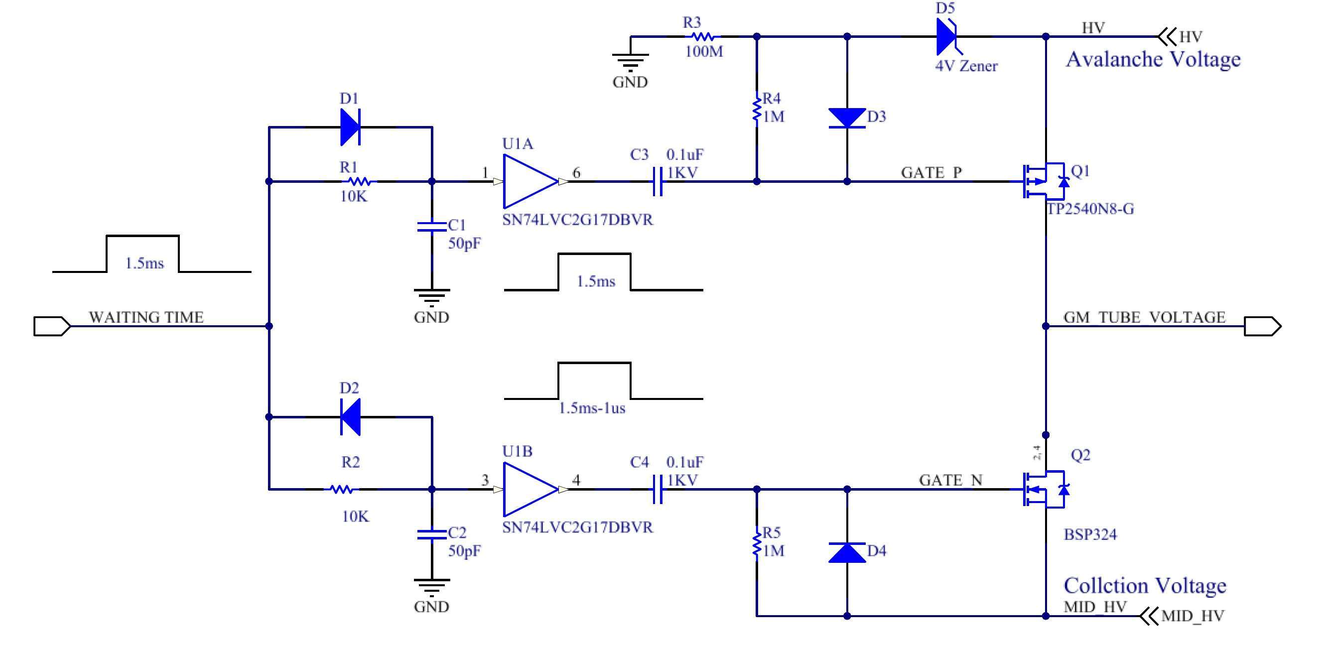
Figure 1 - The practical circuit
The state of MOSFET switches Q1 and Q2 is set by voltage applied to their Gate terminals, relative to the voltage in their Source terminals. The source terminal of Q1 and Q2 are connected to HV of about 600 Volts an MID_HV of about 300 Volts respectively. Capacitors C3 and C4 bridges the gap between low voltage control logic and the high voltages that are needed in the gates. The voltage pulses from the control logic are passed to the transistors gates through the coupling capacitors C3 and C4. A capacitive coupling might cause distortion to the transferred pulses. However, in this case the distortion would be minimal since the time constant of C3*R4 and C4*R5 is 100 milliseconds compared to pulse duration of only 2 milliseconds.
In operational state, Zenner diode D5 and resistor R4 sets Q1 to ON state by applying a voltage of -4V to its Gate, relative to the HV avalanche voltage in its Source terminal. Also in operational state, resistor R5 sets Q2 to OFF state by applying a voltage of 0V to its Gate, relative to the MID_HV Collection Voltage in its Source terminal.
During the waiting 0f 1.5÷2 milliseconds, a positive voltage pulse is be applied to Q1`s Gate. Its VGS is set to zero or positive and it is brought to OFF state. A positive voltage pulse is also applied to Q2`s Gate. It sets Q2 to ON state.
Diodes D3, D4 are placed to restore DC values at the transistors gates.
The roll of timing circuit, consist on R1, C1, D1, R2, C2, D2, is to prevent a state both transistors would be in ON state at same time
Simulation Results
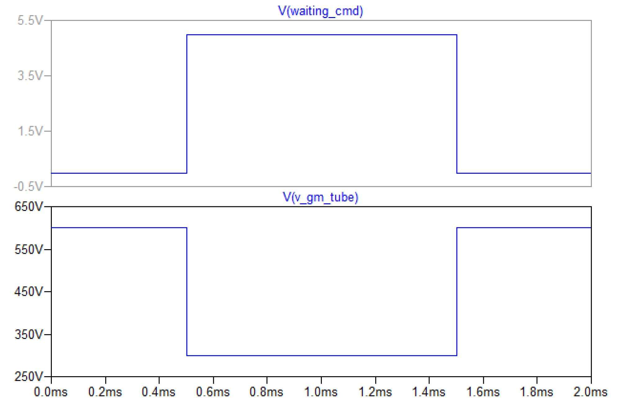
Figure 2- Simulation results
In Figure 2, the simulation shows a voltage switching transfer from 600 Volts to 300 Volts controlled by a 5 Volts logic signal.
Conclusions
- The desirable Switching time achieved with minimal distortion to the pulses.
- Developed a simple and energy efficient circuit to handle high voltage switching in G.M gamma monitors.
- The circuit integrated to operate in radiation monitors time to count mode.
References:
[1] "Radiation Detection and Measurements", G. F. Knoll, 3RD Ed., 2000, pp 214-215
Powered by Eventact EMS