Charge distribution in magnesium aluminate spinel (MAS) results in the formation of a space-charge region, which is then expected to have a critical role in assigning functional properties. Explanations for this phenomenon are reported though quantitative experimental evidence in the case of granular MAS is indirect. To address this topic, we characterized the space charge region in nonstoichiometric nanoscale MAS grains, examining the effect of grain size and applied electric field on the lattice ordering (Fig.1a) and space-charge potential (SCP)[1].
The distribution of cations and point defects [Al••Mg] (inversion parameter) across the grains (Fig.1b) was measured by electron energy-loss spectroscopy (EELS) in scanning transmission electron microscopy (TEM) and compared to the electrostatic potential as measured by off-axis electron holography (EH) in mid-resolution TEM (Fig.1c). We demonstrated quantitatively that regardless of grain size, excess [Al••Mg] defects reside (increased inversion parameter) in the vicinity of grain-surfaces of Al-rich MAS (Fig.1d,e,f). The distribution of electric charge was evaluated by reconstructing the phase shift (Fig.1c) of the electron wave at nanometer-scale resolution. For the same grain, multiple holograms were averaged so that the reconstructed phase was then compared along directions perpendicular to grain surfaces. The contribution of the mean-inner-potential to the phase shifts was evaluated by measuring the relative thickness from the same region using EEL low-loss spectra, as presented in Fig.1d,e,f. Thus, we show that the origin of electrostatic potential difference between the surface and core of the MAS grain is due to the spatial distribution of defects of MAS (Fig.1d,e,f).
We are investigating the effect of grain size on the distribution of the SCP. For grains annealed without applying an external electric field, our measurements show that with decreasing size, the grain core is no longer electrically neutral due to the significant accumulation of charge at surfaces. The effect of an applied electric field on the SCP in MgO∙1.27Al2O3 has also investigation when the grain size, sized ~10nm, is comparable to the Debye length (Fig.1b,d). It has been observed that, while grains subjected to thermal annealing (870°C) show significant charge accumulation (potential above 4V), such grains are subjected additionally to dc-electric fields, up to 1000Vcm-1, and charge accumulation is not detected. Furthermore, since applying a moderate electric field during the annealing process improve lattice ordering (Fig.1a). The origin of this surface charging and its discharge in the presence of an electric field will be discussed.
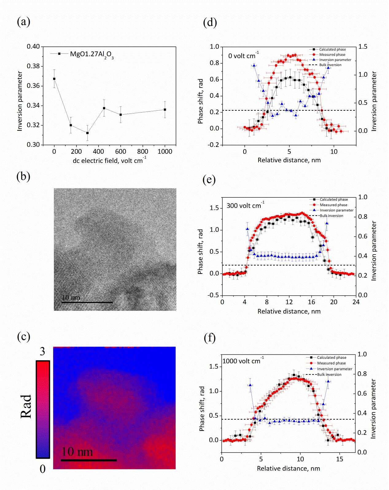
Figure 1. Inversion parameter of MgO•1.27Al2O3 subjected to dc-electric fields, up to 1000Vcm-1, and an annealing temperature of 870°C (a), BF-TEM image (b) and phase-shift map of the electron wave as measured by EH (c) of as-synthesized MAS grains. Line profile values between grain surfaces of the inversion parameter (blue curves), measured phase-shift (red) and, phase-shift calculated from thickness contribution (black) after annealing at 870°C without (d) and with applying an electric field: 300Vcm-1 (e) and 1000Vcm-1 (f)
References:
- Halabi, M. et al., J. Am. Ceram. Soc. 2017;100:800–811.