In the semiconductor industry, the application of Energy Dispersive X-ray spectroscopy (EDS) in the transmission electron microscope (TEM) has been limited to qualitative characterization of devices.
New technology in the form of multiple silicon drift detectors (SDD) with large collection angles, high brightness electron sources and rapid statistical computation of large data sets warrant a reevaluation of this analytical methodology. Our question is whether EDS in the Scanning TEM can enable high-throughput quantitative analysis of ultrathin, beam sensitive films and structures used in advanced integrated circuits.
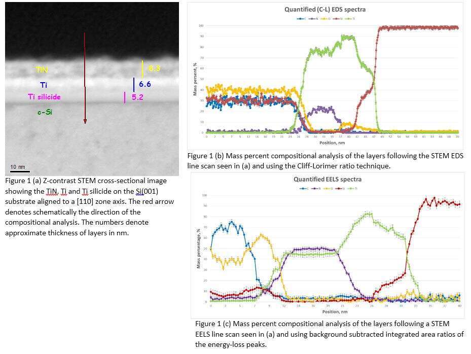
We chose a representative structure on a Si (001) wafer of (thickness in brackets): Ti silicide (5 nm), Ti (6.5 nm), and TiN (8.5 nm) films. We compared between the previous technology of a thermally-assisted field-emission gun (FEG) source with a 0.13srad solid angle Si(Li) detector to a high-brightness FEG source with four SDD detectors collecting X-ray photons from a 0.7srad solid angle [1]. Ultrathin films were prepared both by physical and chemical vapor deposition rendering especially the TiN layer, prepared by the latter method, sensitive to beam damage due to the use of metal-organic compounds.
First, we characterized the onset of electron beam damage to the various layers using an approach described in Refs.[2,3]. These measurements then enabled to define measurement protocols for optimizing X-ray photon count statistics without damaging the layers.
Thus, we utilized the ability of rapid and accurate measurement of the probe current in current TEMs and the sample thickness using a focused ion beam to apply both the Cliff-Lorimer and the Zeta-factor methods for quantitative compositional characterization of the layers.
Quantitative results were compared to electron energy-loss spectroscopy (example in Fig. 1) and X-ray photoelectron spectroscopy measurements. In the case of the TiN layer, energy peak overlaps of X-ray photons from the Ti La and N Ka shells still prohibit their reliable quantitative assessment.
We will discuss the combination of high efficiency SDD with high-brightness FEG source in a STEM as a viable method to enable rapid quantitative EDS analysis of semiconductor devices in the microelectronics industry.
Keywords: Energy dispersive X-ray spectroscopy, Scanning Transmission Electron Microscopy, Microelectronic devices, silicon drift detectors, high brightness field emission electron sources
References:
- FEI Metrios data sheet. http://www.fei.co.jp/_documents/DS0161-02-2014_Metrios-web.pdf
- F. Mansfield, P.R. Okamoto, L.E. Rehn, and N.J. Zaluzec, Radiation effects on X-Ray-microanalysis of a light-element alloy in a medium-voltage electron-microscope, Ultramicroscopy 21 (1987) 13-22
- F. Egerton, F. Wang, and P. A. Crozier, Beam-induced damage to thin specimens in an intense electron probe, Microsc. Microanal. 12 (2006) 65–71