Spintronics exploits the electron spin as an additional degree of freedom in solid state devices, thus enhancing functionalities. Amongst these are novel opto-electronic devices in which injection of perpendicularly spin polarized electrons from a ferromagnetic electrode into a light emitting diode is expected to yield circularly polarized photons [1]. Butler et al. [2] propose that such high polarization electron injection can be achieved in an ultrathin (2-3nm) chemically ordered (B2 or L21) Co2MnSi (CMS) full Heusler due to a combination of perpendicular magnetic anisotropy (PMA) and half-metallicity. PMA is expected due to tetragonal distortion of cubic CMS on epitaxial MgO(001).
Here, we correlate between the structure and magnetic properties of magnetron sputter-deposited ultra-thin CMS electrodes with varying thicknesses and annealing temperatures using transmission electron microscopy (TEM: phase contrast, energy-loss spectroscopy, scanning TEM, HAADF) and magnetometry.
Magnetometry measurements show clear PMA in the ultra-thin layers (Fig.1). Structural characterization using aberration corrected high resolution phase contrast imaging indicates almost complete absence of ordered phases in the CMS layer, consistent with the relatively low magnetic saturation moment (Fig.1). Compositional analysis using sub-nm resolution STEM-EELS indicates chemical intermixing of the Heusler layer with both the MgO and Pd adjacent layers (Fig.2). Consequently, PMA is mostly attributed in this case to interface intermixing anisotropy comparable to Co/Pd multilayers [3] or to Co-Pd alloying [4].
We also note that previous reported structural analyses of these Heusler alloys are undertaken on thin layers (20-50nm), which is then assumed to be comparable in ultra-thin layers (2-3nm). According to our results, this assumption is not valid, and hence these type of ultra-thin film require state-of-the-art TEM analysis.
_magnetic_meas - Copy 2.jpg)
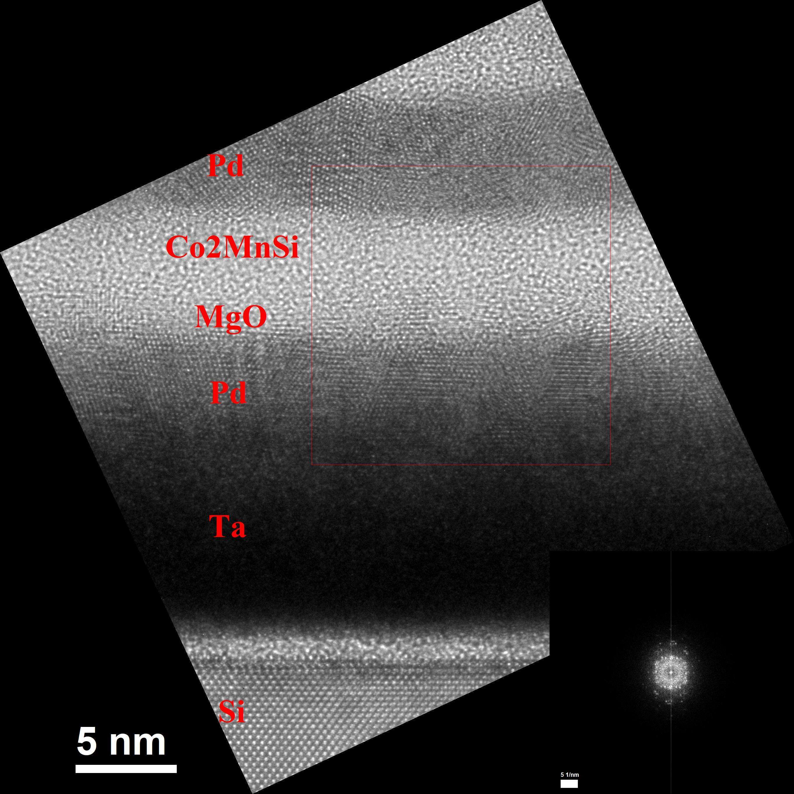
Fig. 1-(Left) M-H loops measured at 300K (SQUID) for sample with Co2MnSi (2.7nm) on top of MgO (2nm) annealed at 350 °C; (Right) Cs corrected HR TEM image (Phase contrast)-(Si Z.A. [110]) (inset: Power spectrum of area denoted by red square).
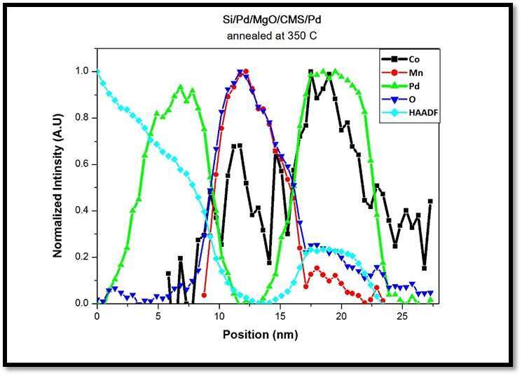
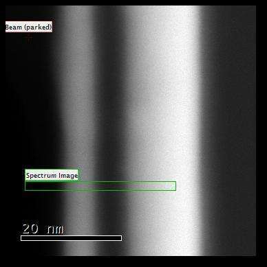
Fig. 2- STEM EELS line scan: (left) Elemental distribution (Right) HAADF STEM cross-sectional image showing area from which EELS line scans were obtained denoted schematically by the green rectangle
1. Farshchi, Rouin, et al., Applied Physics Letters98(16) (2011).
2. Munira, Kamaram, Jonathon Romero, and William H. Butler, Journal of Applied Physics115(17) (2014).
3. Den Broeder, F. J. A., et al., Journal of Applied Physics 61(8) (1987).
4. Shunichi Hashimoto et al., Japanese Journal of Applied Physics 28 1596 (1989).