K. Dicks1, J. Goulden1, P. Trimby1, A. Bewick1
1 Oxford Instruments NanoAnalysis, Halifax Road, High Wycombe, HP12 3SE, UK
CCD-based EBSD detectors have been commercially available for more than 15 years. These detectors are typically either ‘high resolution’ or ‘high speed’. The ‘high resolution’ detectors enable the acquisition of high-quality, megapixel-resolution (>1024x1024 pixels) diffraction patterns with good sensitivity, but limited acquisition speed. Alternatively, ‘high speed’ detectors, typically offer a VGA resolution (maximum 640x480 pixels), with much higher maximum speeds. The latest high-speed CCD-based detectors achieve speeds of ~1500 patterns per second (pps), but only by using extreme pixel binning. This binning has two undesirable effects with regard to pattern quality: a reduction in resolution (only ~40x30 pixels at the highest speed); and a reduction in the maximum signal-to-noise ratio (SNR) before pixel saturation. As a result this high pattern binning compromises analysis, reducing both the hit rate and the orientation precision of fast data acquisition. Not all EBSD applications require a detector’s maximum speed. Some applications require high sensitivity, high resolution and high pattern quality.
The development of a CMOS sensor for EBSD detectors has overcome these issues, delivering a step change in performance. The CMOS sensor architecture enables high speed without the need for extreme, on-sensor binning.
Therefore good resolution and good maximum SNR can be achieved during fast data acquisition. Results from a CMOS-based detector can be collected and analysed in real time at speeds in excess of 3000pps, more than double the speed of any existing CCD-based detector. Importantly, this CMOS detector has a superior maximum SNR and 4x the resolution (16x more pixels) at >3000pps than a CCD detector at ~1500pps (Figure 1). As a result this technology delivers significant improvements to both indexing hit rates and to the angular resolution of orientation measurements.
Optimising angular resolution is important in many EBSD applications, resulting in a significant interest in high resolution (HR) EBSD. This technique uses pattern correlation techniques to compare acquired patterns to reference patterns and to calculate small diffraction pattern shifts[1]. This has enabled analyses with significantly improved angular resolution, when compared to standard Hough-based indexing, with angular accuracies routinely reported below 0.01°.
| |
 |
 |
 |
|
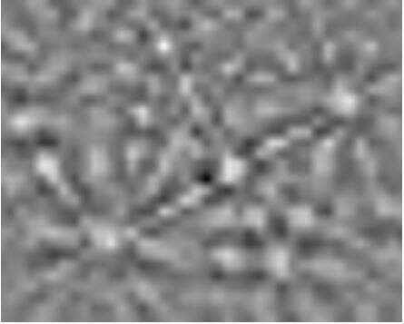
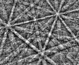
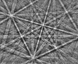
Figure 1 Example EBSPs
|
|
40 x 30 pixel EBSP collected at 1580 pps using a conventional CCD-based detector
|
156 x 128 pixel EBSP collected at 3000 pps using CMOS-based detector
|
1244 x 1024 pixel EBSP collected at 100 pps from a duplex steel sample using a CMOS-based detector
|
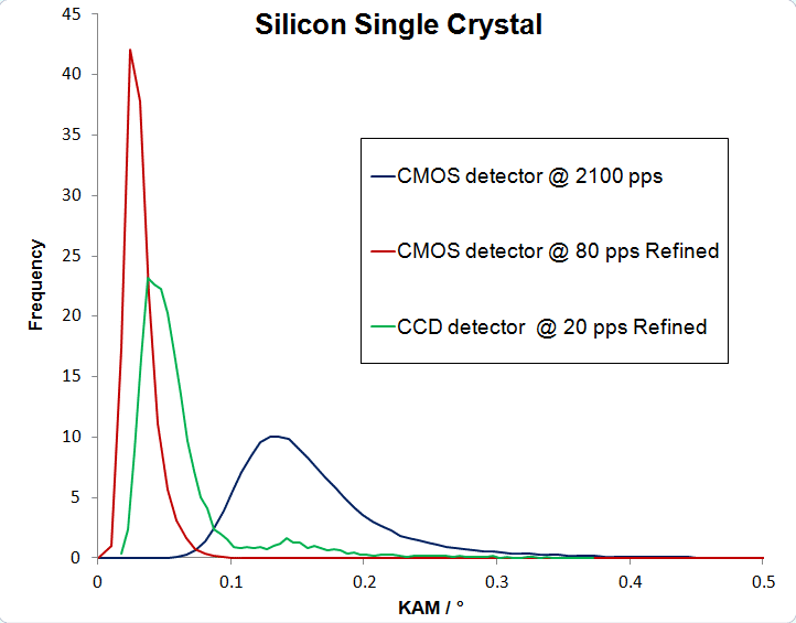
Figure 2. Kernel Average Misorientation distribution plots showing angular accuracy of different analyses / detectors on a Si single crystal. Note the significant improvement in speed and accuracy of a CMOS detector when compared to a CCD detector.
[1] Wilkinson, A. J., Meaden, G. & Dingley, D. J. (2006). Mater. Sci.Technol. 22, 1271–1278
[2] Singh, S., Ram, F. & de Graef, M. (2017). J. Appl. Cryst. 50
[3] Alkorta, J., Marteleur, M. & Jacques, P.J. (2017). Ultramicr. 182, 17-27