")
Margulis Prize:
NANOSTRUCTURING OF ELECTRON BEAMS
In the last century, electron microscopy emerged and evolved as an indispensable tool in pioneering investigations into the nanoscale. The modern electron microscope is a well-developed instrument with various additional devices that enable probing materials in with an abundance of analytical methods. However, this remarkable tool is not restricted to inspection of matter. Several years ago, the field of electron beam shaping emerged; the electron wavefunction is spatially molded as one desires and then interacts with atoms and matter. Shaped beams also provide interesting physics as charged, relativistic particles. In this contribution, I will describe our pioneering works over the past several years.
Treated as a wave, the electron in an electron microscope experiences a phase shift φ when passing through thin films. Assuming a non-magnetic material, this phase shift is directly related to the thickness of the film used1. The phase difference property is wildly employed in advanced experimental instruments, such as phase plates that improve contrast. Taking this idea a step forward, by modulating the thickness of such a material, a veritable “mask” of phase shifts can be fabricated, such that – spatially – the electron beam will acquire a phase shift dependent on its position on the mask, φ(x,y).
The principle of holography was invented by Gabor in 19482 in electron microscopy; it is mainly used today to obtain additional information on investigated materials. Originally, however, the purpose of Gabor’s invention was to provide a means of compensating the inevitable spherical aberration of the microscope’s round lenses. It was quickly adopted and greatly expanded on in light optics, giving birth to computer generated holograms, which were first studied by Brown & Lohmann in 1966 3,4, and today constitute an accomplished field. The theory behind these elements summarizes, in fact, a practical method that relates the spatial phase, φ(x,y), given to a wave in one plane, to the resulting wavepacket shape or intensity pattern, in a conjugate plane.
In our work, we mainly used focused-ion beam milling of Silicon-Nitride films to vary the thickness and control the phase shift, though for suitable applications we also employed electron-beam lithography and thin-film deposition. We thus molded the electron beam into different shapes: we investigated the generation of electron Airy beams5, which appear to propagate on a curved trajectory though no force is present, and electron vortex beams5, which carry orbital angular momentum and are expected to interact with bound electrons in atoms in future experiments. Vortex beams are also desired for observation of magnetic effects by electron energy loss magnetic circular dichroism. We generated nearly-arbitrary holograms6, and measured the electron probe reshaped as the letters “TAU” or an image of the atom model with electrons circling a nucleus, see Fig. 1. We further proceeded to shape the wavepackets not simply in the diffraction plane, but in several adjacent planes, yielding 3D shaped spirals and hotspot lattices7, which may be interesting for particle manipulation in a liquid sample. Shaped beams do not have to be exotic; this technique also allowed us to experimentally correct the spherical aberration of a STEM probe8,9, thereby improving the best resolution of a standard microscope which does not employ commercial aberration correctors, see Fig. 2. We recently summarized and reviewed10 the great advances made over the past several years in this fascinating field, which we expect would continue developing rapidly.
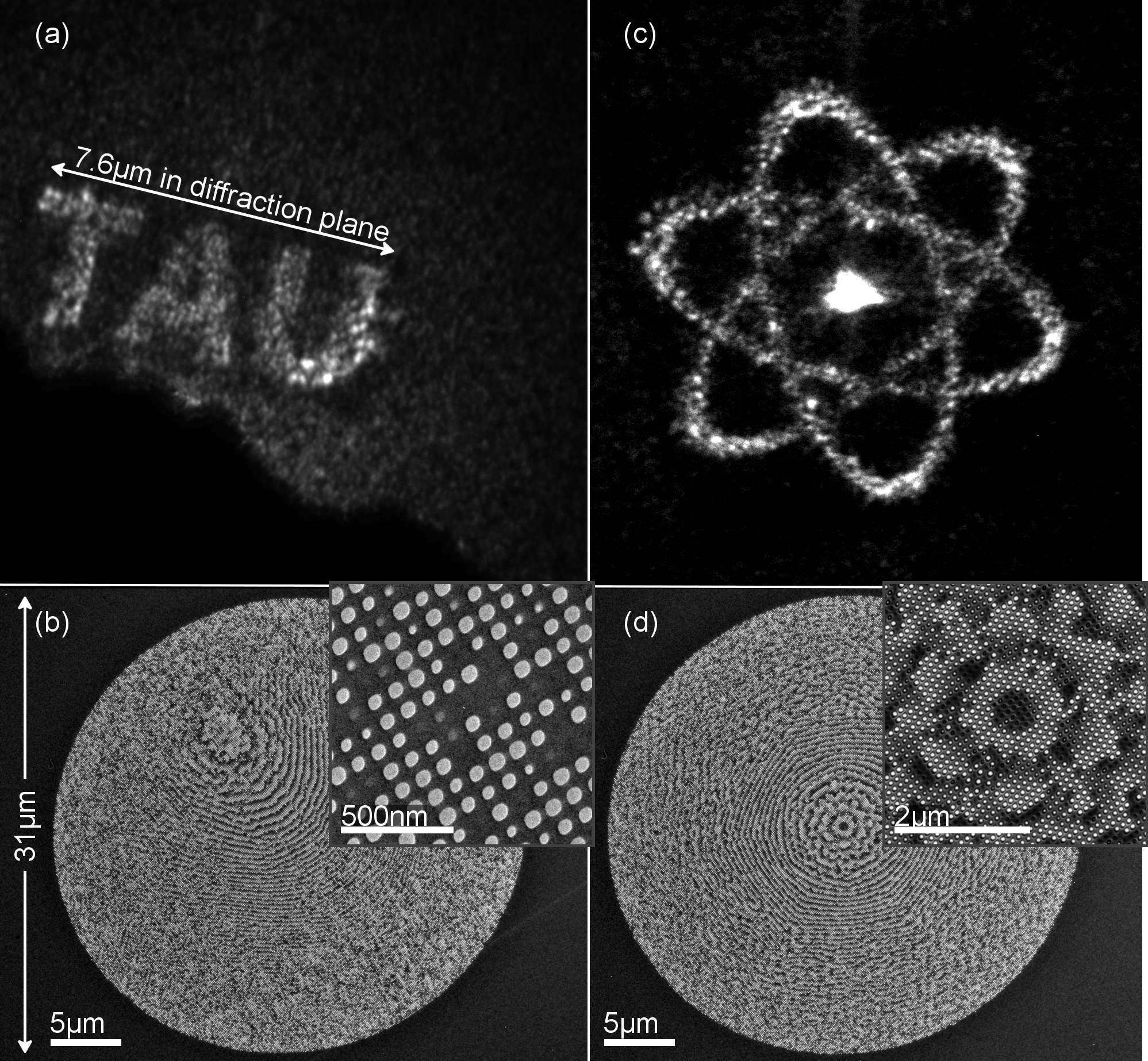 |
Figure 1. On-axis holograms: (a) “TAU” hologram produced by the mask in (b); inset: magnification showing ~60nm holes composing the pixels. (c) Electrons orbiting a nucleus hologram produced by the mask in (d); inset: magnification showing the centre of the mask. | |
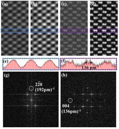 |
Figure 2: HAADF STEM images of Si were recorded without (a,b,e,g) and with (c,d,f,h) the thin film corrector. Images were denoised slightly (b,d) from the raw data (a,c). Intensity profiles of the marked regions in (a,b) and (c,d) are plotted in (e) and (f), respectively, showing the raw data as black lines and denoised data as pink histograms. (g) and (h) show the Fourier spectrum of the unprocessed images (a) and (c). Only after correction does the 136 pm-separated Si dumbbells become visible, both in the HAADF STEM image and in its Fourier spectrum. (a-d) scale bar = 500 pm. |
References:
- Reimer, L. & Kohl, H. Transmission electron microscopy - physics of image formation. (5th edition, Springer, 2008).
- Gabor, D. A new microscopic principle. Nat. 161 777–778 (1948).
- Brown, B. & Lohmann, A. Complex spatial filtering with binary masks. Appl. Opt. 5, 967–969 (1966).
- Lohmann, A. W. & Paris, D. P. Binary Fraunhofer Holograms, Generated by Computer. Appl. Opt. 6, 1739 (1967).
- Shiloh, R. et al. Unveiling the orbital angular momentum and acceleration of electron beams. Phys. Rev. Lett. 114, 1–5 (2015).
- Shiloh, R., Lereah, Y., Lilach, Y. & Arie, A. Sculpturing the electron wave function using nanoscale phase masks. Ultramicroscopy 144, 26–31 (2014).
- Shiloh, R. & Arie, A. 3D shaping of electron beams using amplitude masks. Ultramicroscopy 177, 30–35 (2017).
- Shiloh, R., Remez, R. & Arie, A. Prospects for electron beam aberration correction using sculpted phase masks. Ultramicroscopy 163, (2016).
- Shiloh, R. et al. Spherical aberration correction in a scanning transmission electron microscope using a sculpted thin film. Ultramicroscopy 189, 46–53 (2018).
- Shiloh, R. et al. Nanostructuring of electron beams. Phys. Scripta, Accept. (2018). doi:10.1088/1402-4896/aaf258
Margulis prize: details on my contribution to this work: The project I described naturally involves more than one person. Personally, I designed the experiments, developed code and performed simulations, developed fabrication methods and auxiliary software, fabricated the devices and samples, performed the experiments (except that in ref. 9), and conceived some ideas (particularly ref. 5 and ref. 7). I collaborated with Roei Remez (another PhD student from my grout at TAU) who developed the theoretical model for ref. 5, and designed, developed, and analyzed optical aberrations-related models and theory in refs. 8,9. A second collaborator is Peng-Han Lu (a PhD student at Ernst-Ruska Center, Germany), who performed the experiments in ref. 9.
Powered by Eventact EMS