")
ELECTRON BEAM INDUCED CURRENT AS A TOOL TO INVESTIGATE WORKING MECHANISMS IN HALIDE PEROVSKITE SOLAR CELLS
2School of Energy and Chemical Engineering, UNIST, Ulsan, South Korea
Lead-based halide perovskite (HaP) solar cells, with demonstrated efficiencies >20%, are a potentially valid alternative to existing commercial solar cells.1 These materials, composed of PbI2, PbBr2, methyl ammonium and/or formamidinium and bromide and/or iodide, have a tunable band gap between 1.5 eV and 2.3 eV,2 and depending on their composition their working mechanism can be a p-n or p-i-n junction.3,4
Electron Beam Induced Current (EBIC) is a scanning electron microscope-based method which utilizes the electron beam as a carrier excitation source in order to detect charge separation in a sample. The EBIC signal is a beam-induced current flowing through an external circuit. Unlike the normal operation and analysis of SEM samples, where the beam electrons are led from the sample to the ground, in EBIC a signal will only be detected when electrons and holes are collected at their respective contacts due to a driving force in the form of a p-n or p-i-n junction and energy level mismatches.
EBIC measurements can probe carrier diffusion lengths, Ln and Lp, which is a critical material/device property for solar cells. Here, we use a special form of EBIC, plan-view, on full devices to obtain Ln and Lp, because the width of the active absorber in the devices is less than the diffusion lengths. As this is not the usual way in which EBIC is used to extract diffusion lengths, we detail on how we can use plan-view EBIC and the working assumptions. A model for charge separation mechanism as well as estimates of carrier diffusion lengths can be deduced from EBIC collection efficiency mapping of a photovolatic device, in this case, fluorine-doped tin oxide (FTO)/dense-TiO2/mesoporous (mp)-TiO2/HaP/PTAA (poly triarylamine)/Au. The EBIC measurements were carried out on a representative HaP sample, namely, [FAPbI3]0.85[MAPbBr3]0.15.
Excited carrier diffusion lengths can be determined from EBIC measurements only if the carrier motion is not subject to any electric field, but such lengths can also be derived from the drift lengths. Carrier diffusion and drift are correlated by the Einstein relation, D = μkTq−1, where D is the diffusion length, μ is the carrier mobility, and k, T, and q are the Boltzmann constant, absolute temperature, and carrier charge, respectively. In a p-i-n device, where an electric field is present throughout the absorber film, an upper limit of the diffusion length can be estimated from plan-view EBIC images. There, EBIC mapping is done at the edge of the Au contacts for holes, and at the FTO edge for electrons (Figure 1a,b). To make it possible for carriers to be collected, carrier motion must be perpendicular to the built-in field and we can assume, to a first approximation, that the carrier motion is not affected by the field that exists across the layer (i.e., 90° from the direction of measurement in plan-view). The resulting estimate of the diffusion length is considered as an upper limit, because of the fast extraction of the complementary carrier type to the selective contact. In this case an uneven concentration of excited holes and electrons in an already low-doped semiconductor results in a low recombination rate. In order to estimate excited carrier diffusion lengths, we assume significant lateral transport in the PTAA is unlikely due to its high resistance compared to that of the HaP film. This is due to a 2 to 3 orders of magnitude higher hole mobility in the HaP than in the PTAA and also the difference in the layer thickness (over 500-nm-thick HaP layer and less than 50 nm for the PTAA). Reduced concentration of one type of carrier due to fast extraction of one of the carrier types along with point excitation would increase the effective apparent diffusion length of the other carrier by lowering the probability of second order recombination.
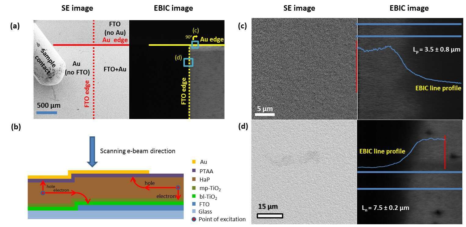
Figure 1. Plan-view images of a device, using secondary electron (SE) contrast (left) and EBIC measurements (right). In all images, the TiO2/HaP/PTAA layers are present. The changes are only in the presence or absence of the electrodes to the selective contacts, FTO or Au. a The edges of the Au pad and FTO are indicated for clarity. The apparent brighter layer close to the Au edge is an artifact of the scan parallel to an interface where charge extraction occurs. The areas that are shown in (c) (turned 90° clockwise) and (d) are indicated as blue squares. b Illustration of the device showing the edges of the FTO and Au electrodes (c) Expanded SE (left) and EBIC (right) images at the Au pad edge of the device, which is rotated by 90 degrees with respect to (a). d Expanded SE (left) and EBIC (right) images at the FTO edge of the device. Owing to coverage by multiple layers, the FTO edge cannot be resolved in the SE image. Using EBIC contrast, the FTO edge can be located clearly.
We find that the EBIC signal is high and constant up to the FTO edge and to the point where the Au layer becomes discontinuous. Beyond these borders, the signal starts to decay, which allows measurement of Ln and Lp diffusion lengths. We can extract the diffusion length from the EBIC data by fitting the EBIC current to a simple exponential decay, Equation (1):
I = I0 + Ae[-X/Ln or Lp] (1)
where I is the signal intensity, I0 is the intensity at maximal collection efficiency, A is an arbitrary intensity coefficient, X is a spatial coordinate and Ln/p is the diffusion length for electrons/holes, as described by Donolato et al.5 The 1-D model, on which Equation (1) is based, assumes that excited carrier motion under neutral field conditions is limited by the diffusion length. In such a model, where the carrier motion is perpendicular to the line across which carrier separation occurs, the current can be modeled by an exponential decay as described by Equation (1). The derived diffusion lengths are Ln = 7.5 ± 0.2 μm and Lp = 3.5 ± 0.8 μm, as shown in Figure 1c, d. The electron diffusion length is longer than the hole diffusion length, as commonly observed in semiconductors with a lighter effective mass of electrons than of holes,6 as was previously found for MAPbI3.3 Analysis of regular, cross-sectional EBIC and beam-damage analysis of the sample shows that adding an excess of PbI2 to the precursors solution yields a material that is less susceptible to defect formation, as well as reduced recombination at the mp-TiO2/HaP interface.7
References:
(1) NREL chart https://www.nrel.gov/pv/assets/images/efficiency-chart.png.
(2) Noh, J. H.; Im, S. H.; Heo, J. H.; Mandal, T. N.; Seok, S. I. Nano Lett. 2013, 13, 1764–1769.
(3) Edri, E.; Kirmayer, S.; Mukhopadhyay, S.; Gartsman, K.; Hodes, G.; Cahen, D. Nat. Commun. 2014, 5, 3461.
(4) Kedem, N.; Brenner, T. M.; Kulbak, M.; Schaefer, N.; Levcenko, S.; Levine, I.; Abou-Ras, D.; Hodes, G.; Cahen, D. J. Phys. Chem. Lett. 2015, 6, 2469–2476.
(5) Donolato, C. J. Appl. Phys. 1989, 66, 4524–4525.
(6) Umari, P.; Mosconi, E.; De Angelis, F. Sci. Rep. 2014, 4, 4467.
(7) Park, B.; Kedem, N.; Kulbak, M.; Lee, D. Y.; Yang, W. S.; Jeon, N. J.; Seo, J.; Kim, G.; Kim, K. J.; Shin, T. J.; et al. Nat. Commun. 2018, 9, 3301.
Powered by Eventact EMS