")
POLYTYPISM IN Cd CHALCOGENIDES THIN FILMS
2Ilse Katz Institute for Nanoscale Science and Technology, Ben-Gurion University of the Negev, Beer-Sheva, Israel
Cd chalcogenide films are direct band gap semiconductors that can harvest photon energy in a wide energy range from 2.42 eV (CdS) to 1.74 eV (CdSe) by compositional tuning or chemical gradation. Growth of such films using chemical solution deposition is advantageous due to low production costs and the ability to easily control bath composition and resulting film microstructure. Due to relatively close Gibbs’ free energy of zinc blende (ZB) and wurtzite (WZ) phases of CdS and CdSe polytypism can be formed.1 In this study we present chemical solution deposition of cadmium chalcogenide thin films with a well-defined orientation relationship with the monocrystalline substrate which allow predicting and controlling orientation and morphology of the films. Moreover, polytypism was observed in the films as high density of stacking faults which follow the film growth orientation.
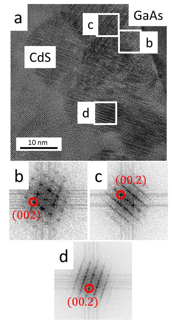
Polytypism was observed in CdS films on GaAs(100) using cross-sectional bright-field high resolution transmission electron microscopy (HR-TEM; Figure 1) . Fast Fourier transform (FFT) analysis showed that the film initiated from (111) faces of CdSZB phase which served as substrates for subsequent CdSWZ growth. Further analysis of the orientation relationships between the film and the substrate conducted by electron diffraction and dark field TEM revealed that the planes in which polytypism is observed are parallel to {111} planes of the GaAs substrate. Moreover, CdS and CdSe monocrystalline films were deposited on GaAs(111) substrates. Analysis of the samples in two 90˚ rotated cross-sectional selected area electron diffraction (SAED) revealed highly defective films in zone axis (ZA) of [110] and defect free films in ZA of [1-10] (Figure 2). This phenomenon is a known visibility condition which indicates that the stacking faults reside in the (111)/(00.1) plane.
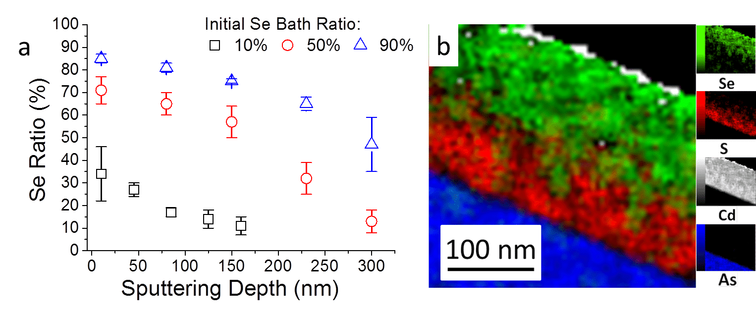
Energy-dispersive X-ray spectroscopy (EDS) was carried out in the scanning transmission electron microscope (STEM) in order to determine selenide concentrations of the films as a function of depth in Cd(S,Se) solid solution films deposited on GaAs(100) substrates. Results from samples with selenide ratios of 10%, 50% and 90% (Figure 3a) showed high selenide content at the film surface, which decreased toward the film-substrate interface. While CdSe has a lower solubility product (Ksp) than CdS (4x10-35 and 10-28, respectively), thiourea decomposes at lower pH value than selenosulfate and as a result the sulfide anions are first to reach and react at the substrate surface. The increase in selenide content toward the films surface is visually demonstrated by the EDS-STEM elemental map in Figure 3b.
- C.-Y. Yeh, Z. Lu, S. Froyen and A. Zunger, Physical Review B, 1992, 46, 10086.
- O. Friedman, A. Upcher, T. Templeman, V. Ezersky and Y. Golan, Journal of Materials Chemistry C, 2017, 5, 1660-1667.
- O. Friedman, D. Korn, V. Ezersky and Y. Golan, CrystEngComm, 2017, 19, 5381-5389.
- O. Friedman, O. Moschovitz and Y. Golan, CrystEngComm, 2018, 20, 5735-5743.
![Figure 2. 90˚ rotated cross-sectional HR-TEM image taken from the interface of monocrystalline CdSe films deposited on GaAs(111)B (As terminated). (a) Highly defective film with SAED inset indicating that the CdSe [110] ZA is parallel to the GaAs [1-10]. (b) Defect free image with SAED inset indicating CdSe [1-10] ZA parallel to GaAs [11-2] ZA.](https://events.eventact.com/duin/31453/Picture2.png)
Powered by Eventact EMS