")
CHARACTERIZATION OF SHORT RANGE ORDER (SRO) IN BEAM SENSITIVE AMORPHOUS LOW-k MATERIALS USING ELECTRON SCATTERING
2Center for Nanoscience and Nanotechnology, Tel Aviv University, Tel Aviv, Israel
The continuous miniaturization of electronic devices over the past decades has led to the challenges of parasitic capacitance, cross-talk and power dissipation between closely adjacent metallization lines separated by a dielectric material. This issue has been addressed by the transition to materials with lower dielectric constant which are developed using various organic and inorganic materials [1].
One of the widely investigated and implemented low-k materials are porous carbon doped silica (SiOCH) due to their compatibility with fabrication processes as well as their thermal properties [2]. The reduction of the dielectric constant is achieved by replacing the highly polarized Si-O bonds with methyl group as well as increasing the porosity of the material [1]. The high porosity leads to poor mechanical properties of the material rendering it vulnerable to plasma patterning processes and to high energy electron beams [3].
Hence, localized structural analysis of such low k material is required for understanding the influence of patterning processes on the dielectric properties at points of interest such as near the metallization lines.
Characterization of the Short Range Order (SRO) in similar types of amorphous materials was previously demonstrated by extracting the Radial Distribution Function (RDF) from electron scattering measurements in TEM [4].
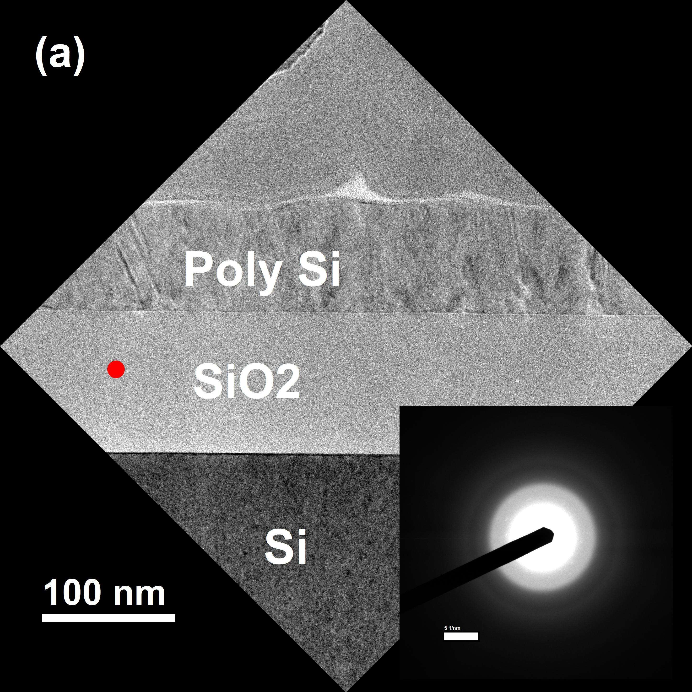
Here we demonstrate a more localized SRO characterization of various beam sensitive amorphous low k films (Fig.1) using low dose electron beam exposures and a correction for the measured modulation transfer function (Fig.2) of the detection system. This combination allows for reduced damage of the dielectric and higher accuracy in determining the structural atomic configuration at points of interest in the device.
[1] Morgen, Michael, et al. "Low dielectric constant materials for ULSI interconnects." Annual Review of Materials Science 30.1 (2000): 645-680.
[2] Maex, Karen, et al. "Low dielectric constant materials for microelectronics." Journal of Applied Physics 93.11 (2003): 8793-8841.
[3] Volksen, W., et al. "Hybrid low dielectric constant thin films for microelectronics." Scripta Materialia 74 (2014): 19-24.
[4] Cockayne, David JH. "The study of nanovolumes of amorphous materials using electron scattering." Annu. Rev. Mater. Res. 37 (2007): 159-187.
 - Copy 1.jpg)
Fig 1. (a) TEM BF image of SiO2 film on Si substrate. Inset: electron diffraction obtained from the area denoted in the red circle. (b) Radial distribution function of SiO2 extracted from the electron scattering measurement.
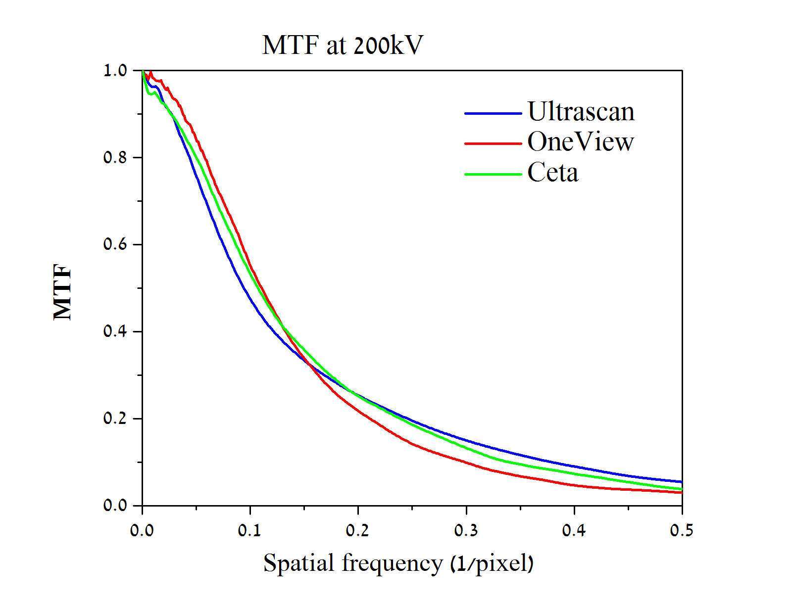
Fig 2. Modulation transfer function of detection systems: FEI CETA, Gatan ONEVIEW and Ultrascan1000.
Powered by Eventact EMS