")
MEAN INNER POTENTIAL OF CRYSTALS- AN ELECTRON HOLOGRAPHY AND AB INITIO STUDY
2The Raymond and Beverly Sackler Center for Computational Molecular and Materials Science, Department of Materials Science and Engineering, Tel Aviv University, Tel Aviv, Israel
3Ilse Katz Institute for Nanoscale Science and Technology, Department of Materials Science and Engineering, Ben-Gurion University of the Negev, Beer Sheva, Israel
4Center for Nanoscience and Nanotechnology, Nanoscience and Nanotechnology, The Hebrew University, Jerusalem, Israel
The Mean Inner Potential (MIP) is defined as the volume averaged electrostatic (Coulomb) potential between a material and vacuum [1]. It is a fundamental material property depending on composition, crystal structure and surfaces, so that it is sensitive to charge-density distributions. As such, the MIP is related to the mean square radius of the electron orbitals and to the orbital diamagnetic susceptibility. Thus, we propose to examine the MIP as a quantitative parameter for chemical bonding in crystals.
Based on off-axis electron holography (OAEH) in the transmission electron microscope (TEM), we measured the MIP at an accuracy of better than 0.4V on wedge samples derived from the gradients of the phase of the electron wave and sample thickness.
Phase gradients were measured using OAEH in the TEM, a method proposed by Dennis Gabor (Nobel Prize in Physics, [2]). This experiment forms an interference pattern, referred to as a hologram, between a reference electron planar-wave propagating through the vacuum and an identical initial wave transmitted through the sample [5]. The recorded hologram enables us to reconstruct the phase difference, ∆ϕ, of the electron wave as a function of sample position, x, in the plane perpendicular to the optic-axis [3, 6, 7], in order to extract the MIP, V0, according to the following equation: 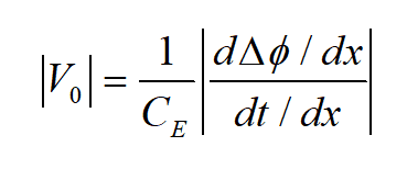
Where CE is the interaction constant, (d∆ϕ/dx) and (dt/dx) are the phase and thickness gradients, respectively.
OAEH offers phase reconstruction at high lateral spatial resolution of several nm over extended regions of interest of hundreds of nm, from sample thickness up to 500 nm [5]. In the absence of dynamical diffraction effects, OAEH is an established method to extract the MIP [3, 4].
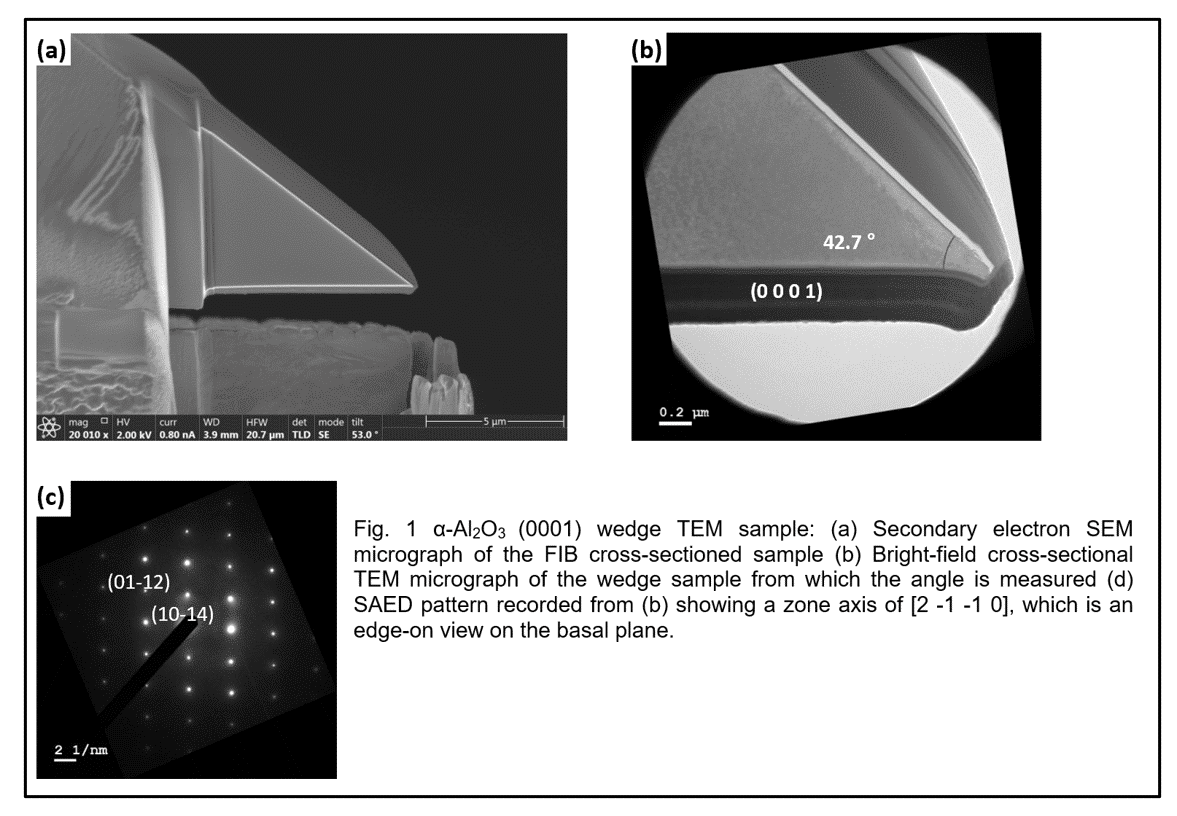
We developed a method to control and measure the thickness gradient of wedge samples with two significant innovations: First, a sample polishing method which can set the wedge angle using a designated mechanical component. Second, the angle (thickness gradient) of the wedge sample was measured to an accuracy of better than 1° by direct observation in the TEM. After the phase measurements, the wedge sample underwent perpendicular sectioning in a focused ion beam (FIB), Fig. (1). Furthermore, the wedge angle was verified independently by a non-destructive approach of confocal optical microscopy.
The viability of our methodology was first demonstrated by measuring the MIP of a Si(001) single crystal, which agreed with reported measured and calculated values.
We then provided the first quantitative MIP determination of sapphire, α-Al2O3(0001): V0 = 16.90 ± 0.36 V. This measurement allows to account for chemical bonding of Al2O3. Using the isolated atom approach to calculate the MIP of sapphire, the electron scattering factors of neutral and ionized Al and O atoms predict upper and lower limits, which can be related to covalent, 19.9 V, and ionic, 15.3 V, bonding, respectively. Following the approach of Peng et al. [8], our MIP measurements determine a 0.66 ± 0.08 fraction of ionic bonds [3].
To account for chemical bonding and for the influence of the crystallographic plane at the surface of the sample, we carried out density functional theory (DFT) calculations [9, 10]. The MIP is extracted as the difference between the potential far from the Al2O3 slab (at the vacuum) and inside the slab, resulting in 15.7 V for the (0001) crystallographic direction. We also performed analogous calculations for a (1–100) crystallographic direction, resulting in a MIP value of 16.7 V, demonstrating a significant influence of surfaces. Notably, our DFT calculation methodology is computationally faster than those reported to date.
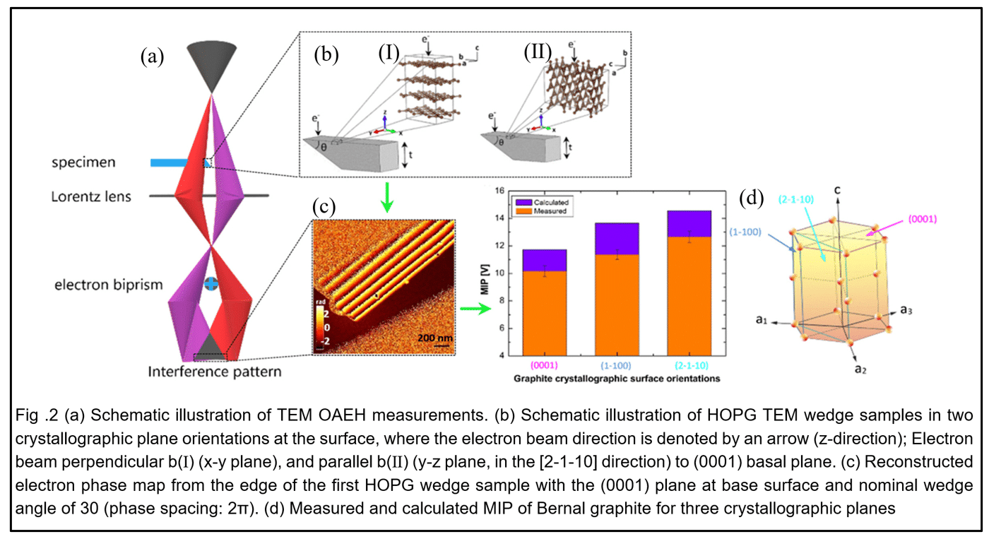
To examine directionality in chemical bonding, we proceeded to an elemental layered crystal, Bernal graphite, which is of significant scientific interest and attracts many technological applications [13]. The choice of a layered crystal, graphite, is because the bonds are anisotropic: strong covalent bonds in eV per atom range within the plane and weak vdW bonds in meV per atom range perpendicular to the basal plane. Wedge samples were prepared from highly-oriented-pyrolytic-graphite (HOPG). Structural examination of HOPG in the TEM showed a high density of basal planar defects of stacking faults and planar rotations around the principal-axis. Consequently, measuring intrinsic properties of an individual Bernal graphite crystal requires probing a volume below 102×102×102 nm3. TEM enabled us to conduct experiments measuring the MIP from such nanometre scale volumes of Bernal graphite oriented, with respect to the electron beam, along the principal axis or along directions in the basal plane. Additionally, these experiments required us to measure accurately the mean-free-path for inelastic scattering in graphite for 197keV fast electrons at a collection angle of 18mrad, resulting in 150.6±2.0 nm.
Thus, we could extract for Bernal graphite crystals with (0001) basal, or (1-100), (2-1-10) prismatic planes, MIP values of 10.16±0.40V, 11.37±0.35V, 12.66±0.41V, respectively [14, 15], see Fig.2. These measured MIP enable to determine anisotropic bonding in the form of the projected mean radii of electron orbitals at 0.704±0.015Å, 0.744±0.015Å, 0.785±0.015Å, respectively. By applying first-principles calculations of crystalline slabs [3], we confirmed these anisotropic measurements with 11.72V, 13.65V, 14.56V, respectively, see Fig.2.
The MIP measurements also enabled to address the unique diamagnetic properties of graphite, which is reported by magnetometry along the principal axis to have the highest susceptibility amongst this class of materials. Our TEM based microstructural characterization of HOPG imply that the large sample volumes required for magnetometry mean that these susceptibility measurements are enhanced significantly by extrinsic signals from basal planar defects [13, 16]. We utilized the relation between the MIP and the diamagnetic orbital volume susceptibility [17], to extract susceptibility values for a defect-free Bernal graphite crystal with (0001) basal, or (1-100), (2-1-10) prismatic planes, of (-1.99±0.08)×10-5, (-2.23±0.07)×10-5, (-2.48±0.08)×10-5, respectively [14].
For the basal plane, an orbital radius of approximately 0.7 Å is consistent with s-bond hybridization [18]. For electron orbitals between basal planes, the larger mean radii in the range between 0.74 Å and 0.79 Å reflect p-bond hybridization of delocalized electrons. Our extracted orbital susceptibilities are comparable to reported magnetometry measurements of diamond, and graphite when the magnetic field is applied perpendicular to the principal axis [19]. However, susceptibility measured by magnetometry with the magnetic field applied along the principal axis is more than an order of magnitude larger. Part of this reported value must originate from a Landau contribution of electrons at basal plane planar defects that we observe in the TEM.