")
METHODOLOGY FOR MEASURING THE ELASTIC AND INELASTIC MEAN FREE PATHS FOR SCATTERING OF FAST ELECTRONS IN TECHNOLOGICALLY IMPORTANT THIN-FILM OXIDES
2Center for Nanoscience and Nanotechnology, Tel Aviv University, Ramat-Aviv, Tel-Aviv, 6997801, Israel
3Andrew and Erna Viterbi Faculty of Electrical and Computer Engineering, Technion - Israel Institute of Technology, Haifa, 3200003, Israel
Thin-film oxides are a primary building block in many devices and have a wide range of applications: optoelectronics, spin-electronics, energy harvesting and storage, memristive devices, and optical coatings [1].
Transmission Electron Microscopy (TEM) is a widely implemented tool for the characterization of such thin films. Quantitative TEM often requires accurate knowledge of sample thickness for determining properties such as: defect density, structure factors, sample dimensions and geometry. Furthermore, an accurate measurement of sample thickness is necessary for modelling image formation, estimation of electron beam or X-ray signal broadening, and radiation damage evaluation.[2], [3].
The most common indirect thickness measurements using Electron Energy Loss Spectroscopy (EELS) can be applied effectively on both crystalline and amorphous materials [2], [4]–[7]. The drawback is that sample thickness is measured in units of inelastic Mean Free Path (MFP).
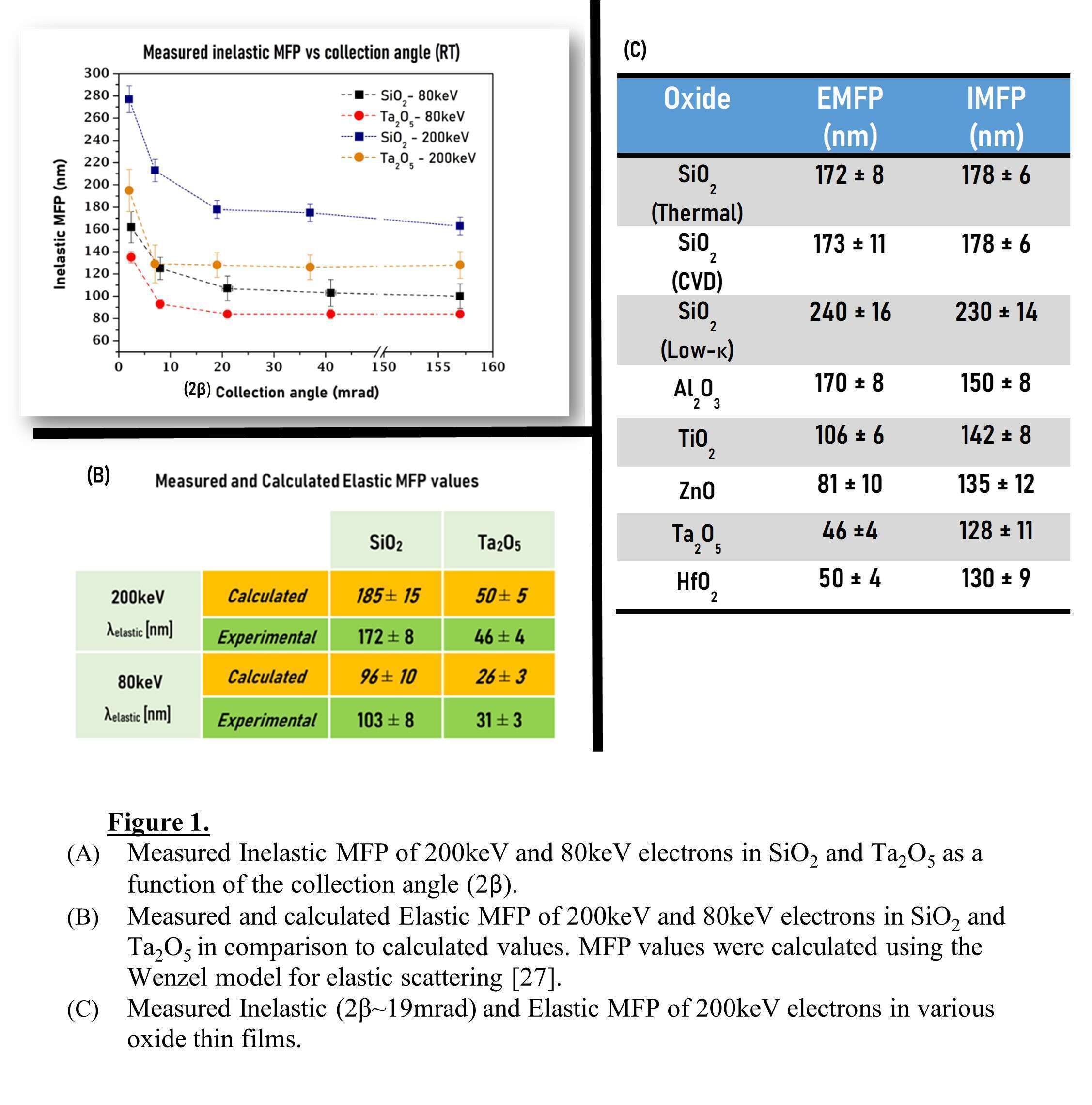
The MFP is measured per material and is dependent on several parameters, for example: Energy of the incident electron beam, and collection angle into the spectrometer. Consequently, to date, MFP values are not reported for many technologically important thin-film oxides.
Furthermore, measuring the Elastic MFP is essential for calculating the optimal sample thickness required for quantitative structural characterizations of amorphous materials (e.g., short-range order) [8].
Hence, a versatile and reliable method is required to enable the extraction of inelastic and elastic MFP values of fast electrons, specifically for thin-film oxides.
In this work we demonstrate a fast and precise method for the extraction of MFP values in oxides thin films grown on Si/SiO2 substrates. The method relies on accurate measurement of inelastic MFP values of electrons in crystalline Si using Energy-Filtered TEM thickness mapping and Focused-Ion-Beam perpendicular cross-sectioning. Using this method, elastic and inelastic MFPs of 80keV and 200keV electrons for technologically important oxides were measured: Ta2O5, HfO2, TiO2, Al2O3, ZnO and SiO2 (thermal/CVD/low-κ) – Fig. (1).
References
[1] M. Kimura, R. Sumida, A. Kurasaki, T. Imai, Y. Takishita, and Y. Nakashima, “Amorphous metal oxide semiconductor thin film, analog memristor, and autonomous local learning for neuromorphic systems,” Sci. Rep., vol. 11, no. 1, p. 580, 2021, doi: 10.1038/s41598-020-79806-w.
[2] K. Oh-ishi and T. Ohsuna, “Inelastic mean free path measurement by STEM-EELS technique using needle-shaped specimen,” Ultramicroscopy, vol. 212, no. December 2019, p. 112955, 2020, doi: 10.1016/j.ultramic.2020.112955.
[3] P. L. Potapov, “The experimental electron mean-free-path in Si under typical (S)TEM conditions,” Ultramicroscopy, vol. 147, pp. 21–24, Dec. 2014, doi: 10.1016/J.ULTRAMIC.2014.05.010.
[4] C. W. Lee, Y. Ikematsu, and D. Shindo, “Measurement of mean free paths for inelastic electron scattering of Si and SiO2,” J. Electron Microsc. (Tokyo)., vol. 51, no. 3, pp. 143–148, 2002, doi: 10.1093/jmicro/51.3.143.
[5] H.-R. Zhang, R. F. Egerton, and M. Malac, “Local thickness measurement through scattering contrast and electron energy-loss spectroscopy,” Micron, vol. 43, pp. 8–15, 2012, doi: 10.1016/j.micron.2011.07.003.
[6] T. Malis, S. C. Cheng, and R. F. Egerton, “EELS log‐ratio technique for specimen‐thickness measurement in the TEM,” J. Electron Microsc. Tech., vol. 8, no. 2, pp. 193–200, 1988, doi: 10.1002/jemt.1060080206.
[7] A. J. Craven, J. Bobynko, B. Sala, and I. MacLaren, “Accurate measurement of absolute experimental inelastic mean free paths and EELS differential cross-sections,” Ultramicroscopy, vol. 170, pp. 113–127, 2016, doi: 10.1016/j.ultramic.2016.08.012.
[8] D. Cockayne, Y. Chen, G. Li, and K. Borisenko, “The technique of RDF of nanovolumes using electron diffraction,” J. Phys. Conf. Ser., vol. 241, 2010, doi: 10.1088/1742-6596/241/1/012006.