")
CATHODOLUMINESCENCE SPECTROSCOPY FOR ADVANCED MATERIAL SCIENCE
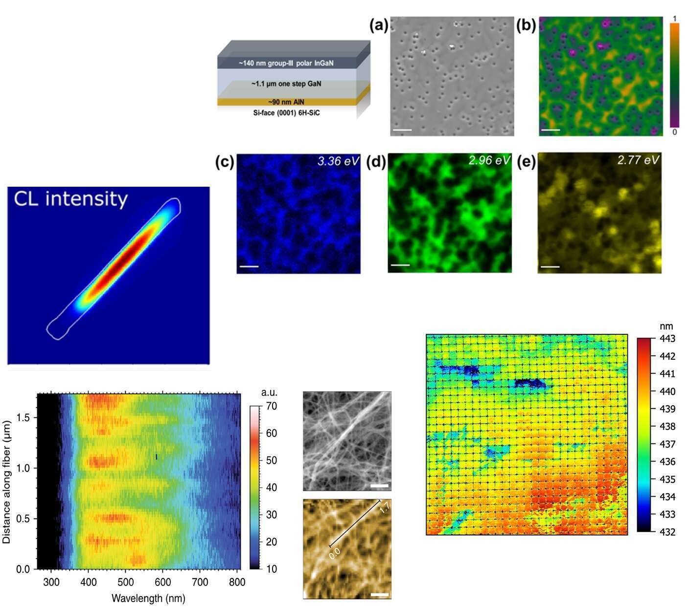
High spatial resolution spectroscopic information may be acquired by using an electron beam in a modern scanning electron microscope (SEM), exploiting a phenomenon called cathodoluminescence (CL) where electrons are promoted from the conduction band to the valence band upon impingement of the high energy electron beam onto a semiconductor. This approach offers several advantages over usual optical spectroscopy techniques. The multimode imaging capabilities of the SEM enable the correlation of optical properties (via CL) with surface morphology (secondary electron mode) at the nanometer scale and the large energy of the electrons allows the excitation of wide-bandgap materials. In addition, CL sensitivity to material composition, as well as the presence of defects, makes it a technique of choice for device characterization.
Quantitative CL has extensively been used to study ageing effects and reliability issues in advanced III-V semi-conductor devices such as nitride-based power devices, light emitting diodes (LEDs) or vertical surface emitting laser (VCSEL) devices. Here, we will present recent advances in instrumental developments as well as recent examples of materials studies.