Mapping tunnelling currents across switchable ferroelectric domains in parallel stacked layered materials with atomic force microscopy
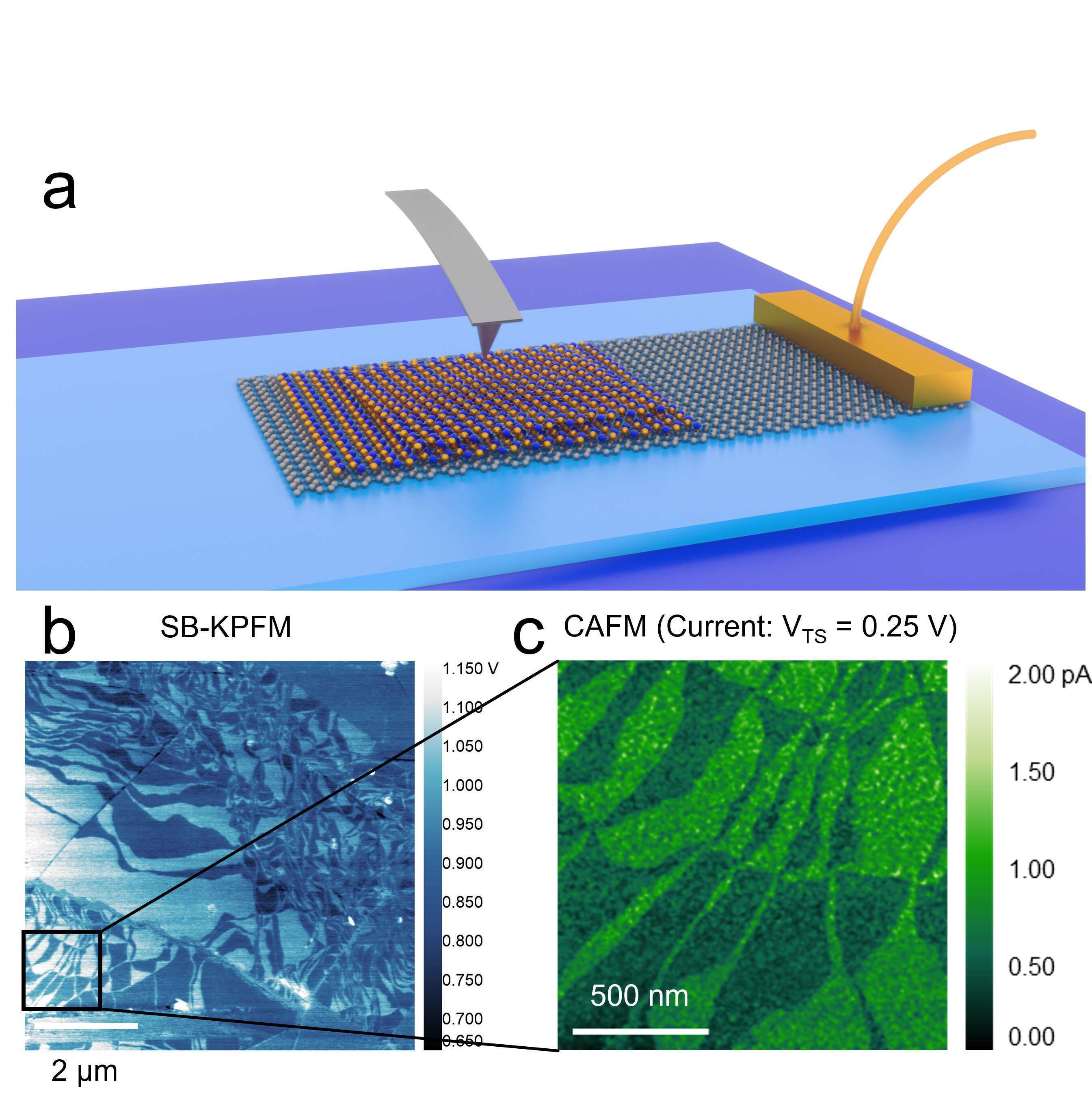
Controlling the twist angle between flakes of layered materials leads to interfacial ferroelectricity in the case of parallel stacked hexagonal boron nitride (hBN) [1-3]. We provide an account of the fabrication of such parallel stacked hBN samples using a home-built transfer setup [4] and the mapping of ferroelectric domains using various scanning probe techniques. We then discuss different ways in which such domains may be mapped and manipulated both electrically and mechanically [3,5]. In particular, we utilise CAFM (where a tunnelling current is measured across a bilayer of parallel stacked hBN) to systematically study the variation of domain morphology versus mechanical setpoint and tip-sample bias.

Fig 1. Parallel stacked hBN may be formed by breaking and restacking exfoliated layers mechanically (a). Once formed, these structures may be characterised using KPFM to map the morphology of ferroelectric domains (b). For sufficiently thin layers (~0.6 nm), tunnelling current may be mapped using CAFM.
We show electrostatically induced switching of the registry of layers, enabling elevated relative areal coverage of AB domains versus BA domains depending upon the magnitude and direction of the applied bias. By performing conductive atomic force microscopy on parallel stacked hBN bilayers on graphene, we simultaneously map and manipulate the superlattice morphology to gain insights into both the mechanics of domain switching and tunnelling mechanisms under the influence of interfacial ferroelectricity. Such measurements are the nanoscale analogue of memristive tunnel diodes formed from parallel stacked hBN, which offer functionalities desirable for ‘more than Moore’ electronic devices.
[1] C. R. Woods et al. Nat Commun. 12, 347 (2021).
[2] K. Yasuda et al. Science 372, 6549 1458 (2021)
[3] M. Vizner Stern et al. Science 372, 6549, 1462, (2021).
[4] Q. Zhao et al. J. Phys. Mater. 3 016001 (2020)
[5] O. Kolosov et al. Phys. Rev. Lett. 74, 4309 (1995)
Powered by Eventact EMS
