Deep Subwavelength Imaging of Gallium Nanoparticle Plasmon Modes
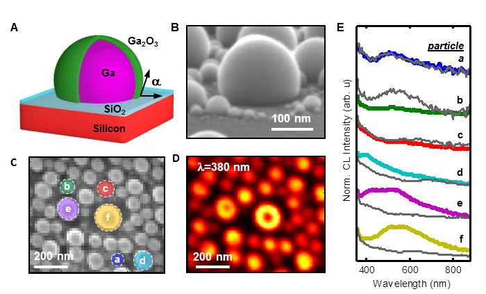
Gallium has recently been demonstrated as a new plasmonic material offering UV tunability, facile synthesis, and a remarkable stability due to its thin, self-terminating native oxide. These properties enable new plasmonic applications, such as simultaneous surface-enhanced Raman spectroscopy, fluorescence, and environmental remediation.[1] The dense irregular nanoparticle (NP) ensembles fabricated by molecular-beam epitaxy make characterization of individual particles challenging; however, such single particle measurements have been a critical factor enabling the explosive growth of noble metal plasmonics. Here we employ hyperspectral cathodoluminescence (CL) microscopy to characterize the response of single Ga NPs within an ensemble characterized by a Gaussian size distribution peaked at a diameter of 72 nm, and with a standard deviation of 15 nm (Fig. 1). We spatially and spectrally resolve both in-plane and out-of-plane plasmonic modes, which can be identified in the CL map as ‘donuts’ and centered peaks, respectively (Fig. 1D,E). These modes, which include both dipole and higher-order terms due to phase retardation and substrate interactions, are correlated with finite difference time domain (FDTD) electrodynamics calculations taking into account the Ga NP contact angle, substrate, and native Ga/Si surface oxidation. This study experimentally demonstrates, for the first time, that single Ga nanoparticles support size-tunable plasmonic resonances with frequency-dependent spatial localization.

Figure 1. Geometry and cathodoluminescence of gallium nanoparticles. (A) Schematic of Ga NP geometry, with (B) a representative scanning electron microscope image taken at 75° tilt. The NP geometry is specified by a contact angle, diameter, and thicknesses of the native particle and substrate oxides. (C) Secondary electron and (D) cathodoluminescence maps simultaneously acquired on a Ga NP array. (E) Spectra taken from the edge (grey lines) and center points (colored lines) for six different particle sizes (a-f: D = 40, 60, 80, 100, 120, 140 nm). Colors correspond to the particles highlighted in (C).
Reference
[1] Y. Yang; J.M. Callahan; T.H. Kim; A.S. Brown; H.O. Everitt. “Ultraviolet Nanoplasmonics: A Demonstration of Surface-Enhanced Raman Spectroscopy, Fluorescence, and Photodegradation Using Gallium Nanoparticles.” Nano Lett. 13, 2837–2841 (2013).
knight@amolf.nl
Powered by Eventact EMS