Monitoring Morphological Changes in 2D Monolayer Semiconductors Using Atom-Thick Plasmonic Nanocavities
Nanometre-sized gaps between plasmonically-coupled adjacent metal nanoparticles enclose extremely-localised optical fields which are strongly enhanced. [1] This enables the dynamic investigation of nanoscopic amounts of material in the gap using optical interrogation. [1-3] Here we use impinging light to directly tune the optical resonances inside the plasmonic nanocavity formed between single gold nanoparticles and a gold surface, filled with only yoctograms of semiconductor.[4] The gold faces are separated by either monolayers of molybdenum disulphide (MoS2) or two-unit-cell thick cadmium selenide (CdSe) nanoplatelets. This extreme confinement produces modes with hundred-fold compressed wavelength, which are exquisitely sensitive to morphology. Infrared scattering spectroscopy reveals how such nanoparticle-on-mirror modes directly trace atomic-scale changes in real time. Instabilities observed in the facets are crucial for applications such as heat-assisted magnetic recording that demand long-lifetime nanoscale plasmonic structures. This spectral sensitivity also allows directly tracking photochemical reactions in these 2-dimensional solids.

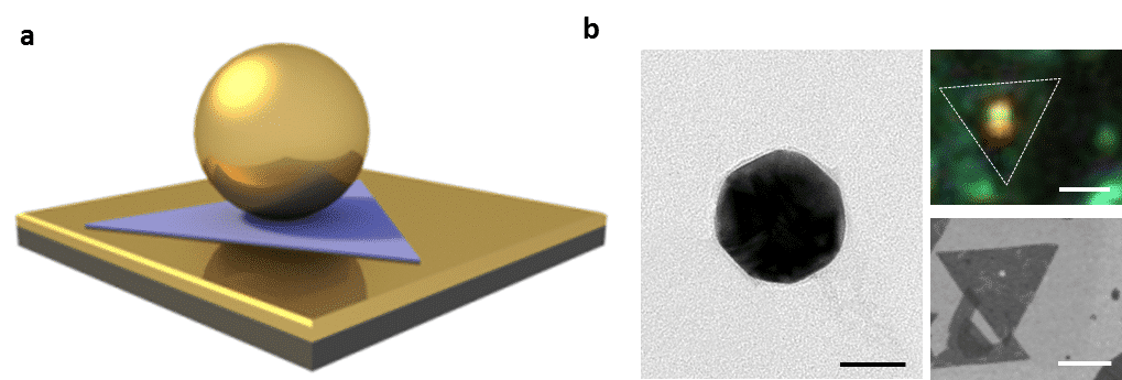
Figure 1: a Geometry utilised: a gold nanoparticle is placed on a semiconductor monolayer on a gold mirror. b Electron microscopy images of a faceted gold nanoparticle, MoS2 platelet and darkfield image showing a gold nanoparticle on a MoS2 platelet.
[1] D.O. Sigle, et al. Phys. Rev. Lett., 113, 1-5 (2014).
[2] J. Mertens, et al. Nano Lett., 13, 5033–5038 (2013).
[3] F. Benz, et al. Nano Lett. accepted, doi:10.1021/nl5041786 (2014).
[4] D.O. Sigle, et al. ACS Nano. accepted, doi: 10.1021/nn5064198 (2014).
jm806@cam.ac.uk
Powered by Eventact EMS