Waveguide-Embedded Modulator for Active Plasmonic Devices
A major goal of active plasmonics is to create a device capable of modulating an input signal. Since surface plasmon polaritons (SPPs) are very sensitive to the properties of the surrounding media, changing the local permittivity of a plasmonic waveguide structure enables the modulation of the output signal. Moreover, the high field confinement permits performing the modulation on nanoscale dimensions.
Here we propose a modulator based on a metal-oxide-semiconductor (MOS) capacitor. Theoretical and experimental [1] studies of such structures have shown a satisfactory modulation depth per unit length at telecommunication wavelengths.
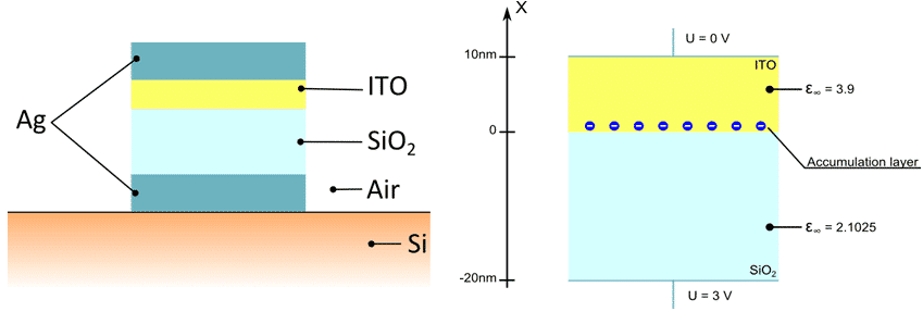
The plasmonic modulator presented here is designed to modulate the propagation of a fully plasmonic mode. The device is embedded on an insulator-metal-insulator (IMI) waveguide structure (FIG. 1) and consists of two metal slabs with dielectric and semiconductor layers between. We use an indium-tin oxide (ITO) as an active material in the modulator.

Applying an external potential to the metallic terminals leads to the accumulation of electrons at the ITO-SiO2 interface. This in turn leads to a local change in the refractive index of the ITO layer. Moreover, the electric field strength inside the ITO layer increases which causes higher attenuation and, thus, a higher modulation depth.

Also, due to the mismatch between the characteristic impedances of the MIM and IMI waveguides the modulator itself forms a Fabry-Perot resonator. This permits increasing the modulation depth even further, since the change of the ITO refractive index shifts the resonance and thus, increases reflection from the modulator.
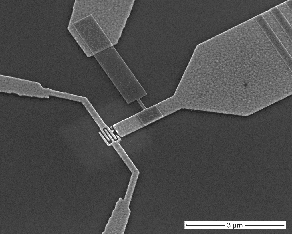
Here we present theoretical and computational analysis of the plasmonic modulator. Progress in experimental studies of a fabricated device (FIG. 2) will also be presented.
References:
[1] Sorger, V et al., Ultra-compact Silicon Nanophotonic Modulator with Broadband Response. Nanophotonics 2012, 1.1, 17-22
epanchenko@student.unimelb.edu.au
Powered by Eventact EMS