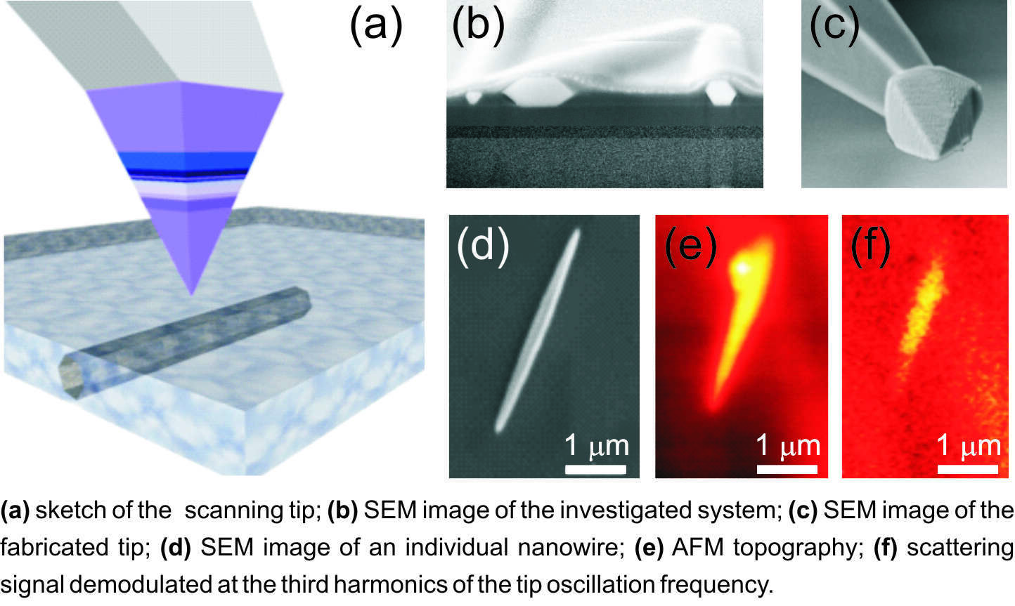
Scanning Probe Tips made of Plasmonic Germanium for Resonant Scattering Imaging of ZnO Nanowires Embedded in a PDMS Matrix
The fabrication of novel scanning probe tips based on electromagnetic design of their plasmonic response has allowed unprecedented resolution and sensitivity in near-field optical microscopy both in the visible [1] and in the mid-infrared (mid-IR) [2] ranges.
In this work, we aim at the high-contrast nanoimaging of composite materials employing mid-IR radiation to achieve substance-specificity. Instead of using metals to obtain the desired plasmonic behavior in the mid-IR, we fabricated tips made of epitaxial semiconductor material with ultra-high doping level above 1019 cm-3. The material of choice was n-doped germanium grown on silicon wafers. The tip fabrication consisted in gluing pyramids of epitaxial material onto flat-hat AFM cantilevers using a focused-ion beam apparatus. TEM images confirm that the crystal quality was preserved during the fabrication steps.
Scattering scanning near-field mid-IR microscopy was performed on ZnO nanowires embedded in a PDMS matrix, a prototype for novel nano-piezo generators, at several electromagnetic frequencies, both above and below the plasma frequency of the Ge tip. Numerical electromagnetic simulations allow understanding the details of the absorption and scattering processes involved.
Work at the Molecular Foundry was performed under User Proposal # 1773. The research leading to these results has received funding from the European Union’s Seventh Framework Programme under grant agreement n°613055. We acknowledge support from Neaspec Gmbh.

[1] Wei Bao, M. Melli, N. Caselli, F. Riboli, D. S. Wiersma, M. Staffaroni, H. Choo, D. F. Ogletree, S. Aloni, J. Bokor, S. Cabrini, F. Intonti, M. B. Salmeron, E. Yablonovitch, P. J. Schuck and A. Weber-Bargioni Science 338, 1317 (2012)
[2] F. Huth, A. Chuvilin, M. Schnell, I. Amenabar, R. Krutokhvostov, S. Lopatin and R. Hillenbrand, Nano Lett. 13, 1065 (2013).
emilie.sakat@polimi.it
Powered by Eventact EMS