An Active-Tuned Plasmonic Modulator by Voltage
Plasmonic modulators controlled by electrical signal have attracted many researchers due to their advantages of being the bridge between electrics and optics, and the compatibility with existing integrated electronic circuits.[1] In this work, we utilized liquid crystal (LC) molecules as a medium to control the extraordinary optical transmission (EOT) of light through a grating structure by applying electrical signals on LC. And the potential application as a wavelength modulation element in a plasmonic laser device was investigated.

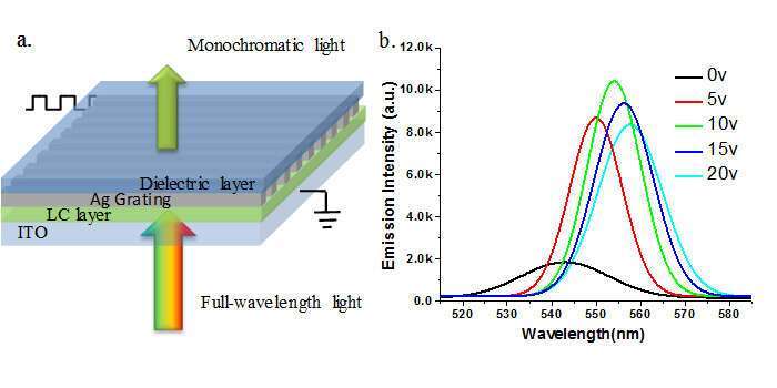
Figure 1 (a) The configuration of the LC-tuned plasmonic modulator based on the EOT mechanism. (b) The emission spectra of SPPs with different voltages applied on LC.
Fig. 1 (a) shows the configuration of the plasmonic mudulator. The key element in the modulator is an Ag double-side gratings, which was obtained by vacuum evaporation deposition of Ag (thickness= 70 nm) above a grating template. Between Ag gratings and ITO, a LC molecule layer (thickness=50 μm) was fabricated by the siphonic effect. When voltage signal (0-20 V) was applied on the Ag gratings and ITO, the rafractive index of the LC layer changed along (from 1.55 to 1.71). On the other side of the Ag grating, we spin-coated a dielectric layer as a refractive index maching layer (n=~1.7). When an normal incident light irradiated on the Ag/LC interface, the surface plasmon polaritons (SPPs) will be excited by a mono-wavelength lightwave with a grating mode, which is sensitive to the refractive index of the liquid crystal layer that can be active-tuned by applied voltage. On the other side of the Ag grating, the same mono-wavelength lightwave will shine out due to the EOT effect. Therefore, a monochromatic beam will radiate to far field. From Fig. 1 (b) that voltage-tuned SPPs emission spectra, we can find that the central wavelength of the SPPs emission shows a red shift with the voltage applied on the LC increasing. This result proves that this plasmonic modulator can be used as a wavelength modulation element when composed with plasmonic laser devices.
Acknowledgements: This work was supported by the National Instrumentation Program (NIP) of MSTC (2011YQ03012408) and NNSFC (21373096).
References:
[1] Lee, H. W., et.al, Nano letters, 14(11),6463-6468 (2014).
xuwq@jlu.edu.cn
Powered by Eventact EMS