Quantitative Angle-Resolved Small-Spot Reflectence Measurements on Plasmonic Perfect Absorbers: Impedance Matching and Disorder Effects
Plasmonic devices with absorbance close to unity have emerged as essential building blocks for a multitude of technological applications ranging from trace gas detection to infrared imaging. A crucial requirement for such elements is the angle independence of the absorptive performance. In this work [1], we develop theoretically and verify experimentally a quantitative model for the angular behavior of plasmonic perfect absorber structures based on an optical impedance matching picture. To achieve this, we utilize a simple and elegant k-space measurement technique to record quantitative angle-resolved reflectance measurements on various perfect absorber structures. Particularly, this method allows quantitative reflectance measurements on samples where only small areas have been nanostructured, for example, by electron-beam lithography. Combining these results with extensive numerical modeling, we find that matching of both the real and imaginary parts of the optical impedance is crucial to obtain perfect absorption over a large angular range. Furthermore, we successfully apply our model to the angular dispersion of perfect absorber geometries with disordered plasmonic elements as a favorable alternative to current array-based designs.

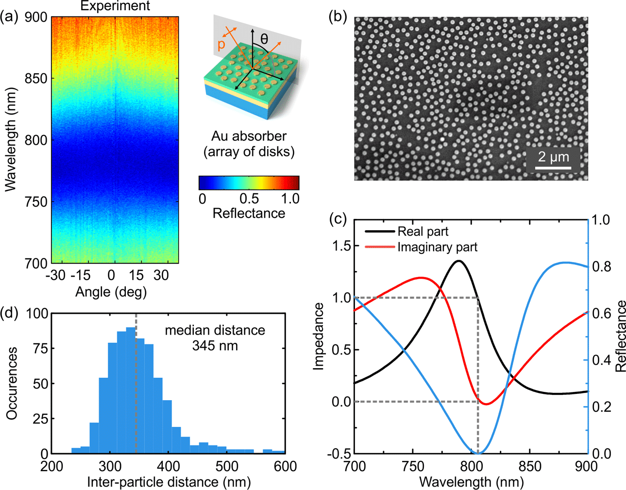
Fig. 1 (a) - Measurement of the reflection as a function of wavelength and angle from a disordered sample. (b) SEM image of the disordered sample. (c) The impedance and the reflection obtained from a FDTD simulation. (d) A histogram of the distance between the different gold nanodisks.
[1] Tittl A., Harats M. G., Walter R., Yin X., Schäferling M., Liu N., Rapaport R., Giessen H., ACS Nano, 2014, 8 (10), pp 10885-10892
moshe.harats@mail.huji.ac.il
Powered by Eventact EMS