A Foundry-Compatible Plasmonic Material Platform Based on Heavily Doped Epitaxial Germanium-on-Silicon
Replacing metals with thin-film semiconductor materials with high carrier density could led to a new generation of plasmonic devices, where plasmonic elements are integrated with standard electronic platforms [1]. In this framework, the most attractive thin-film materials are those whose growth is compatible with silicon foundry processes and silicon substrates. One notable example is electron-doped germanium (n-Ge), which features a small effective mass of 0.12 and supports heavy doping levels up to 3×1019 cm-3 hence allowing plasma frequencies up to the mid-infrared range.
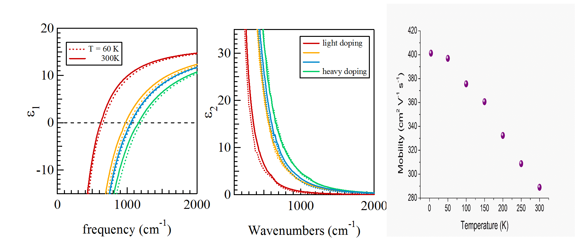
In this work, we measured the optical and electrical transport properties of n-Ge thin films hetero-epitaxially grown on silicon substrates by plasma-enhanced chemical vapor deposition (PE-CVD). From normal-incidence reflectivity measurements and Hall-transport data taken on the as-grown materials as a function of temperature and dopant incorporation levels, we derived a phenomenological model of electron scattering from optical and acoustic phonons, charged impurities (donors and charged dislocations) and neutral impurities (crystal defects and neutral disclocations). The Kramers-Kronig relations were finally employed to calculate the complex dielectric function directly from the optical data in a model-free fashion, in order to perform electromagnetic simulations of plasmonic devices.
The research leading to these results has received funding from the European Union’s Seventh Framework Programme under grant agreement n°613055.
[1] G. V. Naik, V. M. Shalaev and A. Boltasseva, Advanced Materials 25, 3264 (2013)

giliberti.valeria@gmail.com
Powered by Eventact EMS