Laser Printing of Silicon Nanoparticles with Unique Optical Properties
Silicon nanoparticles with controlled shapes and sizes can be used in novel nanophotonic components such as nanolasers [1], sensors [2] and metamaterials [3]. For this purpose, a suitable printing method allowing the generation and arrangement of these nanoparticles in a very precise manner is needed.
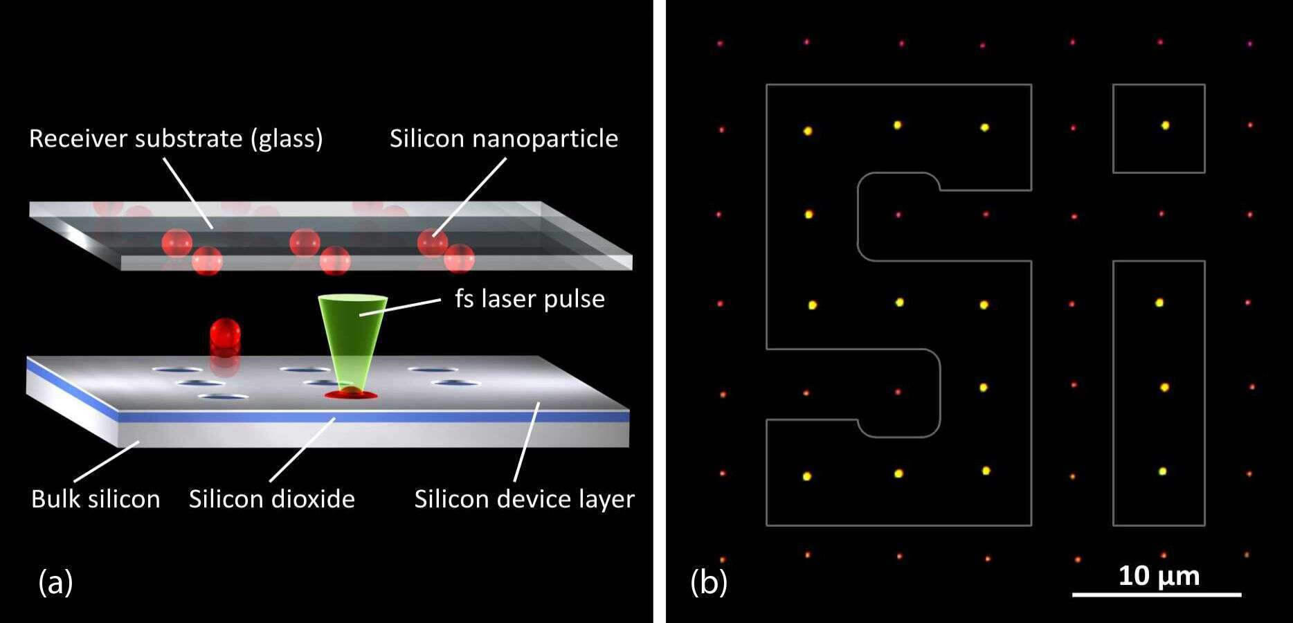
At the Laser Zentrum Hannover we developed a novel laser printing technique for the controlled fabrication and precise deposition of spherical silicon nanoparticles [4]. Using femtosecond laser pulses it is possible to vary the size of Si nanoparticles and their crystallographic phase. The generated silicon nanoparticles with sizes of a few hundred nanometres exhibit unique optical properties due to their strong electric and magnetic dipole responses in the visible range. The novel fabrication technology allows the generation of individual amorphous and crystalline spherical Si nanoparticles with precisely controlled optical properties. The laser-printed nanoparticles are initially in amorphous phase (a-Si). By additional single-pulse laser irradiation, the amorphous nanoparticles can be controllably transformed into crystalline particles (c-Si) or into particles with more complex mixed amorphous/crystalline phases. This technology provides unique possibilities for laser tuning of optical properties of individual Si nanoparticles.

Figure 1. (a) Schematic illustration of femtosecond laser printing of nanoparticles. A silicon-on-insulator (SOI) wafer was used as a target to transfer spherical Si nanoparticles from a 50nm crystalline Si layer onto the transparent glass receiver substrate. (b) Dark-field microscopic image of the laser-printed Si nanoparticles. The nanoparticles within the white lines are crystallized by additional laser pulse irradiation, producing a visible colour change [4].
References
[1] Baranov, D. G., A. P. Vinogradov, and A. A. Lisyansky. "All-dielectric nanolaser." arXiv preprint arXiv:1408.5164 (2014).
[2] García-Cámara, Braulio, et al. "Sensing with magnetic dipolar resonances in semiconductor nanospheres." Optics express 21.20 (2013): 23007-23020.
[3] Shi, Lei, et al. "A New Dielectric Metamaterial Building Block with a Strong Magnetic Response in the Sub‐1.5‐Micrometer Region: Silicon Colloid Nanocavities." Advanced Materials 24.44 (2012): 5934-5938.
[4] U. Zywietz, C. Reinhardt, A.B. Evlyukhin, B.N. Chichkov, „Laser printing of silicon nanoparticles with resonant optical electric and magnetic responses“, Nature Communications, 5, No. 3402, (2014).
U.Zywietz@lzh.de
Powered by Eventact EMS