Directional Emission of Electron-Beam-Driven Plasmonic Nanostructures
The ability to control the directivity of light emission from single nanoscale emitters such as quantum dots or fluorescent molecules has made plasmonic nanoantennas one of the key elements in nanophotonics. Here we demonstrate that the wavefront of light emanating from such ‘point sources’ can be manipulated by locating them in a holographically designed nanostructured environment enabling the conversion of basic dipole radiation patterns into virtually any desired wavefront (e.g. a directional plane wave or an optical vortex beam).
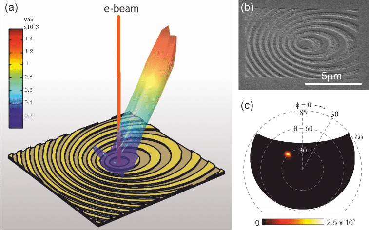
In the present study we utilize the impact point of a free electron beam on a plasmonic metal surface as the singular, highly localized source. Such impacts generate transition radiation with a dipolar emission distribution and surface plasmons propagating with cylindrical symmetry away from the excitation point. For a given desired far-field output wavefront, the requisite holographic pattern is obtained computationally using the near-field distribution of an electric dipole above a metal surface as a reference beam. Figure 1a shows a model nanostructure designed to produce a plane wave with an output polar angle of 30º at a wavelength of 800 nm.
 |
|
Figure 1: (a) Far-field radiation pattern from electron impact on a holographic mask designed to generate a plane wave at 30º to the surface normal. (b) Scanning electron microscope image of the above mask on a gold substrate. (c) Polar plot of 800 nm light emission from the above hologram mask. |
Figure 1b shows the realization of this computer-generated holographic nanostructure, by focused ion beam milling, on an optically thick gold substrate. The spectral and spatial distribution of electron-induced light emission from the structure is analysed in a scanning electron microscope equipped with angle-resolved cathodoluminescence imaging capability. Figure 1c present the 800 nm light emission distribution for electron injection on at the centre of the holographic nanostructure, showing strongly directional emission at θ~30° as per the design of Fig. 1a.
This demonstration uses a plasmonic metal substrate but the approach can be adapted at the holographic design stage to a variety of nanostructured metal, semiconductor and dielectric environments for highly localized emitters. Further results on generating more complicated wavefronts, e.g. optical vortex beam, will also be discussed.
niz@orc.soton.ac.uk
Powered by Eventact EMS