Low-Loss, Fabrication-Tolerant, TM-Pass Polarizer Based on Hybrid Plasmonic Waveguide
Plasmonics has a potential to help the miniaturization and integration of the photonic devices for telecommunications. However, its practical usage has always been controversial because the plasmon photonic devices are usually lossy and difficult to fabricate. One promising approach is hybrid integration that using plasmonics in functional devices and dielectrics for propagation and connection.
Over the past years, our group has developed a series of novel approaches and constructed a few compact and practical plasmon photonic devices for telecommunications, such as wavelength demultiplexing [1], Band-pass plasmonic slot filter [2], polarization beam splitters [3], and polarization rotators [4]. Polarization handling is an essential issue in telecommunication [5]. While traditional polarization handling devices using dielectric structures which have large size or complicated geometries, we believe that plasmonics, with natural polarization sensitivity and good confinement, will surely help to develop better devices for telecommunication.
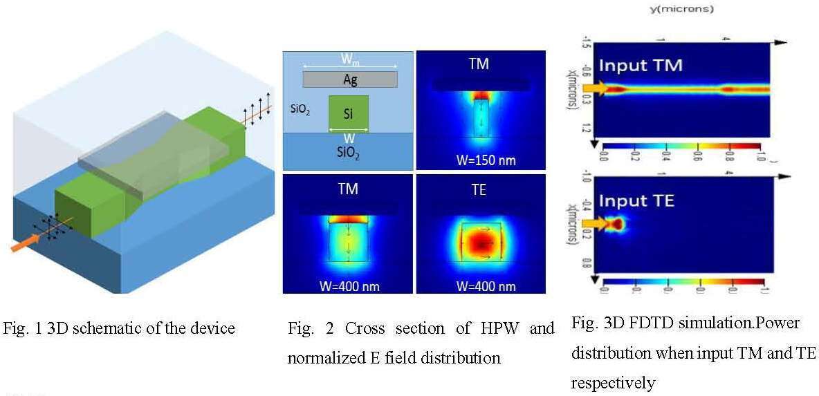
Here we propose a low-loss, fabrication-tolerant, and compact TM-pass polarizer based on hybrid plasmonic waveguide (HPW). As shown in Fig. 1, a narrow HPW (consists of Si wire, SiO2 gap and metal cap) as the polarizer is seamless connected with standard Si wire input/output waveguides through taper couplers. At a small Si width, TE mode in HPW is cut off while TM mode still survives because its plasmonic property. Therefore, the narrow HPW acts as a TM-pass filter. Notably, the metal strip here is wider than Si wire and can be alignment-free during the fabrication, avoiding the biggest challenge in traditional HPW that requires precise alignment between metal and Si waveguide. Moreover, wider metal helps increase TE mode loss and reduce TM mode loss, thus enhances extinction ratio (ER). Fig. 2 and 3 show the simulation results of a 4 μm-long device, from which we obtain ER is higher than 18 dB, while TM insertion loss is only 0.66 dB. The experiment is underway and we expect to show the results at the conference.

References
[1] F Hu, H Yi, Z Zhou, Optics letters 36 (8), 1500-1502
[2] F Hu, H Yi, Z Zhou, Optics express 19 (6), 4848-4855
[3] L. Gao, Z. Zhou, et al, Appl. Phys. B, 113, 199, 2013
[4] L. Gao, Y. Huo, J. S. Harris and Z. Zhou, IEEE Photonic. Tech. Lett., 25, 2081, 2013
[5] T. Barwicz, H.I. Smith, et al, Nat. Photonics,1, 57, 2007
zjzhou@pku.edu.cn
Powered by Eventact EMS