Near Field Direct Demonstration of Super-Resolution Using Silicon Planar Waveguide
Planar Silicon waveguides provide up to 4 times wavelength compression, enabling super-resolution optical microscopy for visible light. We use the following platform to support guided short wavelength guided modes that enable coupling into a near-field scatterer for detection: 100 nm thick Silicon waveguide atop a 200nm metallic mask separated by a 20nm thick SiO2. The waveguide is illuminated with red laser light (671nm), and coupled to the guided modes by thin slits, curved so as to focus the mode. We use a scattering type scanning near-field microscope (s-SNOM) to directly map the near field of the guided modes in the waveguide. A pseudo heterodyne detection method provides background-free amplitude and phase information.
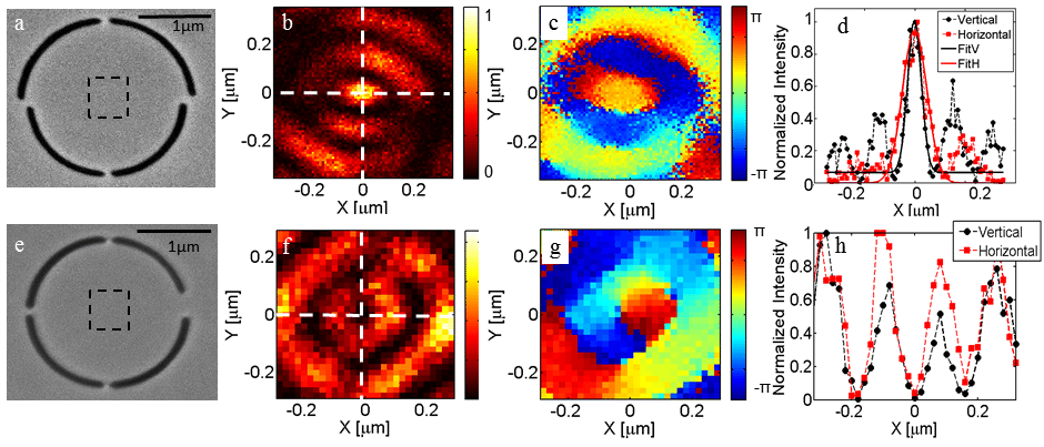
The lenses we used to focus the short wavelength modes are presented in figure 1. First, we used two concentric arcs of circles with a radius mismatch of (Fig 1a-d) that create a bright spot. A close-up high-resolution intensity and phase mapping of the measured near-field normal component Ez is shown in Fig. 1b-c. The line-cuts of the beam along x and y (Fig. 1d) show full width half maximum (FWHM) of 65 ± 5 nm and 115 ± 5 nm, respectively. A different excitation, utilizing circularly polarized light incident upon a circular lens, reveals a planar vortex beam with a dark spot in the middle and spiraling phase (shown in Fig.1 e-h). Such phenomenon has been shown for plasmons on a gold-air interface, but the phase pattern is measured here for the first time. A circular dark spot of 80 ± 15nm radius was measured.
The combination of the focusing abilities demonstrated with an imaging scheme has the potential for a Silicon based next generation microscopy technique.

bgjonaj@ee.technion.ac.il
Powered by Eventact EMS