Hot Electron Schottky Detection Based on Internal Photoemission in Silicon Structures
Silicon is the material of choice in the semiconductor industry. Silicon has a bandgap of 1.1 eV and thus it is transparent above a wavelength of ~1micron. This is why silicon can guide and concentrate light at infrared wavelengths, but it is not efficient in absorbing the infra-red light and converting it into a measurable photocurrent. In spite of the above, there are several approaches for the realization of a silicon based IR detectors, e.g. by using a non-linear processes, defect mediated processes or by integrating silicon with an active layer of germanium or III/V. An alternative way to detect the infrared light in silicon is by using a plasmonic enchanted Internal Photo Emission (IPE) process in a Schottky barrier. Simply, when a semiconductor is attached to the metal, it creates a Schottky contact with a barrier height which is typically lower than the energy bandgap of silicon. Conduction electrons in the metal can absorb photons from the semiconductor with energy higher than the Schottky barrier, cross over the Schottky barrier into the semiconductor and be collected as photocurrent.
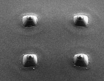
To improve the efficiency of the IPE process we have recently introduced a pyramid shaped structure. In this work we present a comparison between the pyramid shaped devices and flat type devices that were fabricated on silicon chip as shown in Figure 1.

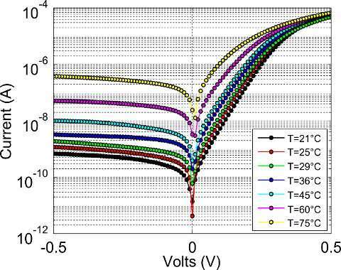
The fabricated devices were characterized by measuring the I-V curves in the dark and under illumination at visible and near IR wavelengths. A typical IV temperature dependent measurement results is shown in Fig.2a. In the infrared spectrum (photon energy below the bandgap of the silicon) there is no contribution of direct electron hole pair generation because silicon is transparent at this regime.

In the talk we will present additional simulations, fabrication and experimental measurement results demonstrating the comparison between different Schottky structures.
dboriska@gmail.com
Powered by Eventact EMS