Nanoscale Tailored Plasmonic Topography for Optimum Broadband Solar Harvesting
This presentation addresses the question: Is it possible to design a dedicated nanostructure on which all surface features contribute entirely to energy harvesting within a solar cell?
This is an important challenge in the light that the efficiency of the solar cell technology utilised has a direct impact on the required land-use and also on reaching grid parity. Techniques that produce efficiencies in excess of the Shockley-Queisser limit (SQL, 32%), including multi-junction cells are still prohibitively expensive. Plasmonic excitation, specifically the enhancement of the electromagnetic field via the excitation of collective electron oscillations in conductive media, has been named at the forefront of technologies which can be applied to existing single and multijunction solar cells and have the potential to even break the SQL when combined with optically non-linear responding materials. This begs the question as to why this has not yet occurred? The answer lies in a fundamental rethinking of plasmonic material design. As traditional plasmonic structures, such as gratings, are not designed with broadband excitation in mind, their integration within an existing solar cell device does not yield a system that contributes completely to absorption enhancement across the harvestable range of wavelengths.

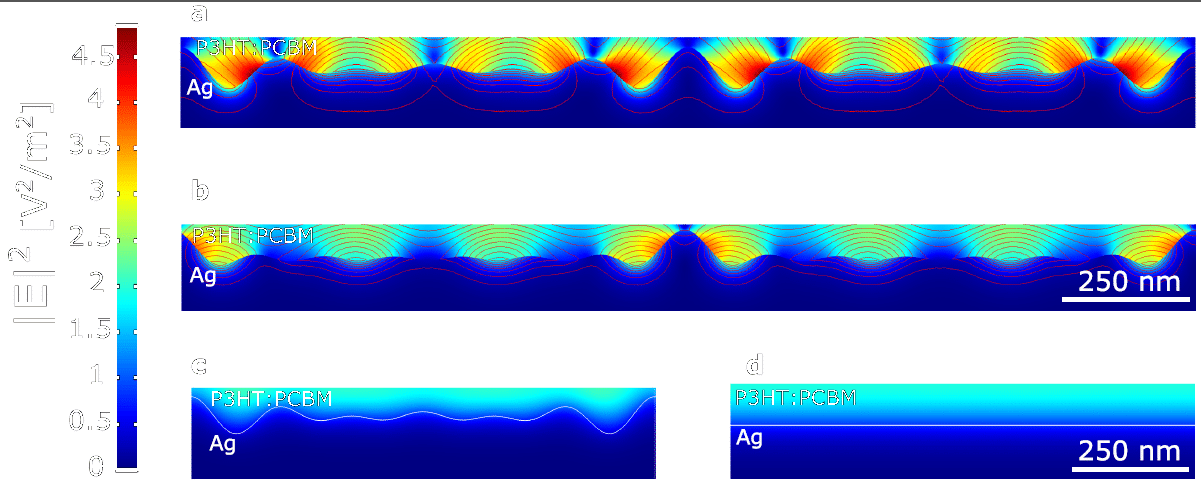
Fig. 1 Field distribution in the vicinity of the nanoscale topography.
Here, we take an unique approach and present an analytically derived optimum solution to the problem: a nanoscale metal topography, capable of significantly improving the efficiency of solid state solar cells via excitation of surface plasmon polaritons (SPPs). The presented structure is designed to achieve broadband excitation of SPPs through the highest possible density of desired k-vectors at the interface. This leads to high weighted absorption enhancements (> 130%) and unprecedented improvements (> 30%) of solar cell external quantum efficiencies over the entire harvestable range.
dominic.zerulla@ucd.ie
Powered by Eventact EMS