Plasmonic Structures with Spatially Varying of Conductivity using Inkjet Printing Technique
Conventional plasmonic materials are typically fabricated using a single homogenous metal and structured to obtain useful functionality. Alternatively, structures are occasionally made in which several homogenous materials are deposited using a layer-by-layer process, such as metal-dielectric-metal structures [1]. However additional control over the propagation properties of surface plasmon-polaritons should be possible if the metal conductivity could also be varied spatially. This is not straightforward using conventional microfabrication techniques.
We demonstrate the ability to vary the conductivity spatially using a conventional inkjet printer, yielding either step-wise changes or continuous changes in the conductivity. We accomplish this using a commercially available inkjet printer, where one inkjet cartridge is filled with conductive silver ink and a second cartridge is filled with resistive carbon ink. By varying the fractional amounts of the two inks in each printed dot, we can spatially vary the conductivity. The silver ink has a DC conductivity that is only a factor of six lower than the bulk silver, while the carbon ink acts as a lossy dielectric at terahertz frequencies. Both inks sinter immediately after being printed on a treated PET transparency.

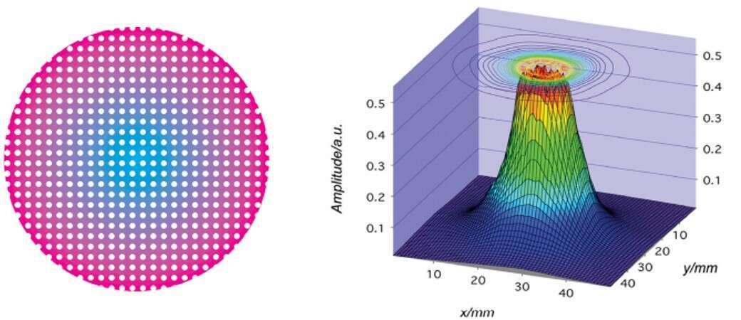
In the left figure, we show a hole array (white circles are holes), where the conductivity varies from 50% Ag/50% carbon (cyan) to 100% Ag (magenta). The periodic aperture consists of 450 µm diameter apertures with a periodicity of 1mm. The figure at right shows the measured beam profile, which shows that the conductivity variation alters the input Gaussian beam profile to a flat top Gaussian with 1/e beam diameter that increases by a factor of 1.7.
References
[1]. Gupta, B., Pandey, S., Guruswamy, S. & Nahata, A. Terahertz Plasmonic Structures Based on Spatially Varying Conductivities. Advanced Optical Materials 2, 565–571 (2014).
ajay.nahata@utah.edu
Powered by Eventact EMS