Heating and Cooling in Electrically Pumped Plasmonic Structures
Metal-semiconductor plasmonic waveguides provide strong mode confinement and are considered to be prospective candidates for on-chip interconnects. However, very short propagation lengths prevent their practical utilization. This limitation can be overcome by compensating for ohmic losses in the metal by optical gain in the adjacent semiconductor. For chip scale integration, pumping and plasmonic waveguides must be integrated on a single chip, which can be achieved with electron and hole injection into the active semiconductor region of the active plasmonic structure. However, inspite of the high efficiency of electrical pumping, the current density approaches 10kA/cm2 in the regime of full loss compensation, which corresponds to a power consumption per unit waveguide length per unit waveguide width of about 5 kW/cm2. It is not difficult to see that this value greatly exceeds the average heat generation of the microprocessor chip (~100W/cm2). This can cause heating of the active region and reduce the device performance or even destroy it.
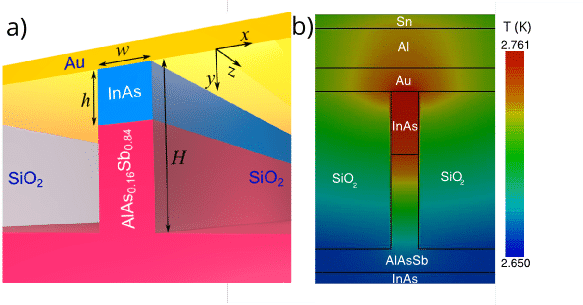
In this work, we study heating and cooling of the electrically pumped active plasmonic waveguide (see fig. 1a). Device is placed under 500 nm layer of Al followed by the 150μm of solder and 1-mm-thick Al bulk. Solving self-consistently the electron and hole transport equations together with the thermal conductivity equation, we find the temperature distribution in the active InAs region. In the regime of full loss compensation, at an average waveguides spatial density of 17 mm-1, electrical pumping does not heat the device: the temperature nearby the Au/InAs contact is only 2.8 K above the ambient temperature (fig. 1b). As the SPP power increases to 10 mW, the maximum temperature increases up to 54 K above the ambient temperature due to the substantial increase in the current density required for full loss compensation. At a practical SPP power of 0.2-1mW, the waveguide heating is very small and can be neglected.

Fig. 1. (a) Schematic of the active plasmonic waveguide. (b) Temperature distribution (with respect to the ambient temperature) in the waveguide cross-section at a low SPP power.
Powered by Eventact EMS