Experimental Demonstration of CMOS-Compatible Long-Range Dielectric-Loaded Surface Plasmon-Polariton Waveguides (LR-DLSPPWs)
A major obstacle of plasmonic waveguides [1-2] is their limited propagation length. Hybrid photonic-plasmonic waveguides were proposed and demonstrated, providing longer propagation length at the expense of weaker mode confinement [3]. Specifically, the long-range dielectric-loaded surface plasmon-polariton waveguide (LR-DLSPPW) [4] offers decent propagation length together with wavelength scale mode confinement. By generating a symmetric-like dielectric environment above and below a thin metal stripe, a long range mode is supported [5]. In this work we demonstrate the design, fabrication and experimental characterization of a high refractive index, CMOS compatible LR-DLSPPWs. The LR-DLSPPW configuration is designed to operate around 1.55 micron wavelength. Our LR-DLSPPW (Fig. 1) consists of a Si3N4 ridge deposited on top of a thin aluminum (Al) strip, which is supported by oxidized silicon-on-insulator (SOI) wafer. Figure.1 (a) presents simplified schematics of the device configuration, while Fig. 1(b) shows the device geometry, which is the result of our fabrication process as can be seen in the SEM image (Fig. 1(c)).

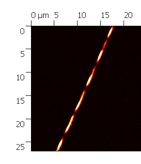
From spectral transmission measurements we have concluded that the propagation loss of the fundamental LR-DLSPPW mode (Fig. 1(d)) is ~6 dB/mm, which is comparable to previously published results, with the estimated mode confinement being ~0.5mm2. Furthermore, we have measured the mode profile using a near field scanning optical microscope (Fig. 2). The near field data show a beat pattern, from which we extract the effective indices of the two modes supported by the structure. The results will be reported in details and discussed during the presentation. We will also point out further research opportunities which can be supported by the reported waveguide platform.

- K. Gramotnev and S. I. Bozhevolnyi, "Plasmonics beyond the diffraction limit," Nat. Photonics 4, 83-91 (2010).
- I. Bozhevolnyi, V. S. Volkov, E. Devaux, J.Y. Laluet, and T. W. Ebbesen, "Channel plasmon subwavelength waveguide components including interferometers and ring resonators," Nature 440, 508-511 (2006).
- Goykhman, B. Desiatov, and U. Levy, "Experimental demonstration of locally oxidized hybrid silicon-plasmonic waveguide," Appl. Phys. Lett. 97(14), 141106 (2010).
- S. Volkov, Z. Han, M. G. Nielsen, K. Leosson, H. Keshmiri, J. Gosciniak, O. Albrektsen, and S. I. Bozhevolnyi, “Long-range dielectric-loaded surface plasmon polariton waveguides operating at telecommunication wavelengths,” Opt. Lett. 36(21), 4278–4280 (2011).
- Sarid “Long-Range Surface-Plasma Waves on Very Thin Metal Films,” Phys. Rev. Lett. 47, 1927-1930 (1981).
roy.zektzer@mail.huji.ac.il
Powered by Eventact EMS