Integrated On-Chip Silicon Plasmonic Four Quadrant Detector for Near Infrared Light
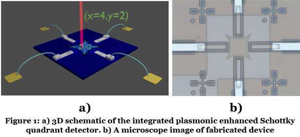
The field of integrated plasmonic devices has become a widespread research topic with applications in physics, engineering, chemistry, biology, medicine, material science and more. Further development of plasmonic applications relies on the capability of integrating advanced passive and active plasmonic devices that can control and detect the propagation of plasmonic fields. For example, directional beaming, splitting, and focusing of plasmonic signals are prerequisites for plasmonic circuitry and plasmonic sensing applications [1]. To date, such capabilities were demonstrated by several groups, and future work is expected to yield even better devices. In this work, we demonstrate the integration of plasmonic coupling, splitting, focusing and detection functionalities in a single device. Our device consist of coupling, splitting and focusing sections [2] that can couple a near infrared light coming from free space to SPPs propagating towards specific desired spatial positions. At these specific spatial locations, Internal Photoemission (IPE) Schottky photodetectors are integrated. These photodetectors convert the sub bangap energy SPP modes into a measured electrical current [3]. A potential application for the proposed device is a four quadrant detector, capable of tracing and tracking the spatial position of an optical beam. A schematic of the proposed structure is presented in Fig 1a.

In this scheme, the light is impinging at the surface from above and couples to SPPs by the slits. To avoid the polarization dependency of SPPs, a circular polarized light was used. Due to the parabolic shape of the slit, the generated SPPs are being focused as they propagate away from the slit. At the focal point of the parabolic plasmonic lens the SPP waves are coupled to an integrated on-chip Schottky photodiode by plasmonic grating couplers. In Fig. 1b an optical image of a typical fabricated device is shown.
References
[1] Liu, Z., Steele, J. M., Lee, H. & Zhang, X. “Tuning the focus of a plasmonic lens by the incident angle”, Appl. Phys. Lett. 88, 171108 (2006).
[2] Lerman, G., and Levy, U, "Pin Cushion Plasmonic Device for Polarization Beam Splitting, Focusing, and Beam Position Estimation", Nano Lett., (2013).
[3] Goykhman, I., Desiatov, B., Khurgin, J., Shappir, J. & Levy, U. “Locally Oxidized Silicon Surface-Plasmon Schottky Detector for Telecom Regime,” Nano Lett. 11, 2219–2224 (2011).
meir.grajower@mail.huji.ac.il
Powered by Eventact EMS