Nonlocal Quantum Simulation of Active Plasmonic Devices Based on Transparent Conducting Oxides
A nonlocal quantum approach for the simulation of active plasmonic devices based on transparent conducting oxides (TCOs) is presented in this work. Our computations show why current theoretical predictions were too optimistic and might explain why experimental findings still lag behind.
In our simulations, the quasi-static electrical and the dynamic optical properties are simultaneously computed. We use Thomas-Fermi theory to determine the carrier accumulation in the TCO when applying a voltage. This carrier density profile is then coupled to the optical properties via a Drude model. The obtained strongly changing inhomogeneous permittivity is resolved by a high order finite element solver. The resulting modes show very sharp features caused by the carrier modulation around the epsilon-near-zero region.
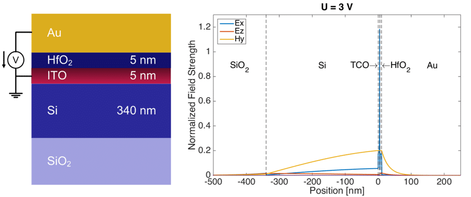
A hybrid plasmonic absorption modulator shall serve as an insightful example. We compare the two most commonly used models in literature with ours. Current research [1-5] assumes a constant carrier density over an accumulation layer inside the TCO which can be tuned to an optimal point of maximal extinction. But such an averaging process perverts the fact that carrier accumulation is exponential. In fact, the high absorption in the epsilon-near-zero region is a very sharp feature. Our model fully resolves this feature and predicts an extinction ratio which is an order of magnitude lower. The corresponding structure and mode are shown in Figure 1.

Figure 1: Structure and mode profile of a hybrid plasmonic waveguide when a voltage of 3 V is applied between the TCO and gold.
[1] A. Melikyan, et al., Opt. Express 19, 8855-8869 (2011).
[2] V. E. Babicheva, et al., Opt. Express 21, 27326-27337 (2013).
[3] C. Ye, et al., IEEE J. Sel. Top. Quant. Electron. 20, 40-49 (2014).
[4] S. Zhu, et al., Opt. Express 22, 17930-17947 (2014).
[5] H. W. Lee, et al., Nano Lett 14, 6463-6468 (2014).
uelikoch@gmx.ch
Powered by Eventact EMS