Optical Modes in Graphene on Silicon Photonic Crystal Membrane
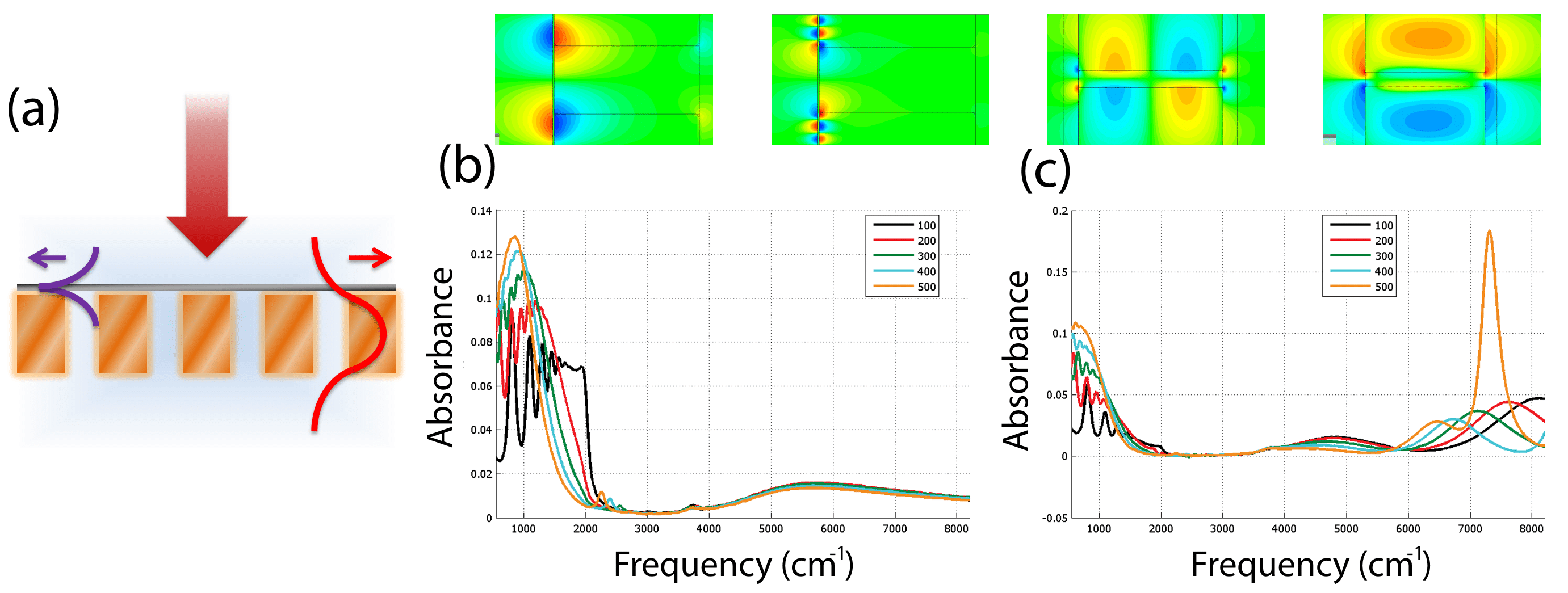
We report on investigation of optical modes in graphene suspended on a silicon photonic crystal membrane [Fig. 1(a)]. Depending on the relations between the structure period a, the graphene surface plasmon polaritons wavelength λSPP, the silicon membrane effective wavelength λphot and the free-space wavelength λ0 (typically λSPP<λphot<λ0) we identify the following regimes of an electromagnetic wave interaction with the structure: (1) metamaterial a<λSPP, (2) plasmonic λSPP<a<λphot, (3) photonic λphot<a<λ0 and (4) diffraction grating regime λ0<a. We study numerically a 1D silicon grating with graphene and absorbance of the normally incident wave [see resonances in absorbance in Fig. 1 (b) and (c)] with variation of geometrical and material parameters. Increasing the period of the grating leads to smearing of the distinct plasmonic peaks into a broad resonance. We also discuss potential strategies for absorbance maximization. Graphene on silicon photonic crystal is a promising platform for terahertz and infrared absorbers, filters, sensors and photodetectors [1, 2].

Figure 1. (a) Normally incident electromagnetic wave can excite plasmonic modes in graphene as well as photonic modes in silicon grating. Simulated absorbance spectrum for the 100 nm (b) and 500 nm (c) thick silicon membrane and graphene’s EF= 0.3 eV for the period a = 100 – 500 nm. Insets show examples of the fields of plasmonic (two left figure, at low frequencies) and photonic (two right figures, at high frequencies) modes.
References
[1] T. Low, and P. Avouris, Graphene plasmonics for terahertz to mid-infrared applications, ACS Nano, 2014 vol. 8, pp. 1086–1101.
[2] Q. Bao, and K.P. Loh Graphene photonics, plasmonics, and broadband optoelectronic devices, ACS Nano, 2012, vol. 6, pp. 3677–94.
Powered by Eventact EMS