Wafer-Scale Photonic and Plasmonic Crystal Sensors
200 mm diameter wafer-scale fabrication, metrology, and optical modeling results will be reviewed for surface plasmon resonance (SPR) sensors based on 2D metallic nano-dome and nano-hole arrays (NHA) as well as 1D photonic crystal sensors based on leaky-waveguide mode resonance, with potential applications in label free sensing, surface enhanced Raman spectroscopy (SERS), and surface-enhanced fluorescence spectroscopy (SEFS). Potential markets include micro-arrays for medical diagnostics, forensic testing, environmental monitoring, and food safety.
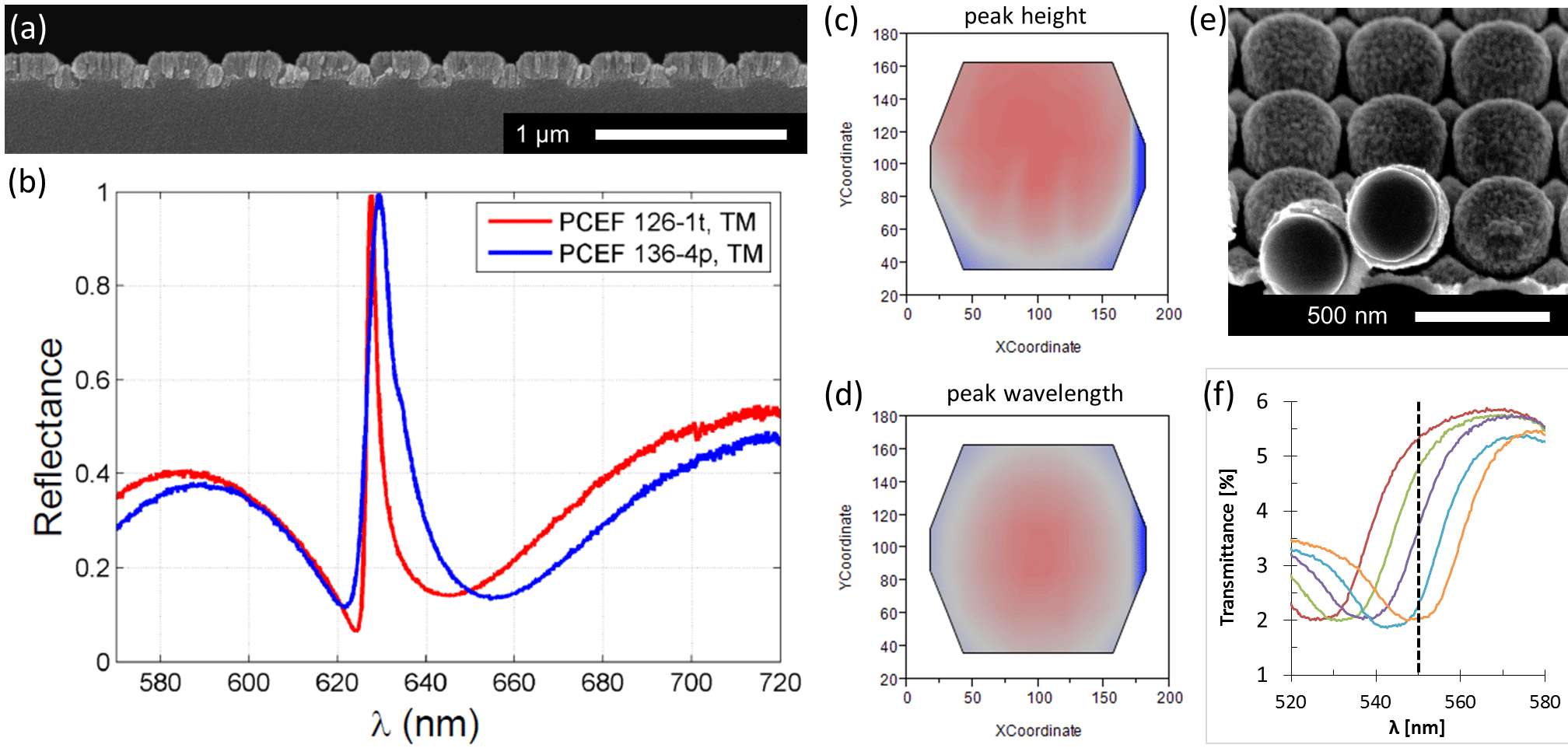
Wafer-scale optical metrology results will be compared to FDTD modeling and presented along with application-based performance results, including label-free plasmonic and photonic crystal sensing of both surface binding kinetics and bulk refractive index changes. In addition, SERS and SEFS results from a line scan microscope system will be presented for several 1D photonic crystal and 2D metallic array structures. Figure 1 presents fabrication and optical metrology results for various 1D and 2D photonic crystal and SPR sensors. Narrow-band photonic crystal resonance sensors showed quality factors over 200, although wafer-uniformity needs further improvement. Gold-coated nano-dome arrays for SERS applications showed gaps with spacing in the 10-20 nm range. Normal incidence extraordinary optical transmission (EOT) results for a 550 nm pitch nano-hole array showed good bulk refractive index sensitivity, however an intensity-based design with 665 nm pitch was chosen for use as a compact, label-free sensor at both 650 and 632.8 nm wavelengths. The optimized NHA sensor gives an SPR shift of about 480 nm per refractive index unit when detecting a series of 0-40% glucose solutions.

Figure 1. (a)-(d) Results for narrow band 1D photonic crystal sensors composed of TiO2 layer on SiO2 grating. (a) SEM cross-section, (b) normal incidence Reflectance, and 200mm diameter wafer maps for 7.5° reflectance showing (c) peak height and (d) peak wavelength uniformity. Red color corresponds to larger Reflectance or longer λ. (e) Au-coated nano-dome array sample. (f) EOT at normal incidence for 550 nm pitch NHA under 0-40% aqueous glucose solutions.
Powered by Eventact EMS