Electrically Pumped Coherent Surface Plasmon Polariton Source Integrated on a Chip
Implementation of optical components in microprocessors can boost their performance by many orders of magnitude. At the same time, the size of optical elements is fundamentally limited by diffraction, which creates a large mismatch between the scales of photonic and electronic components, and it is a significant challenge to merge these two technologies on a single chip.
Metals exhibit negative permittivity at optical frequencies, which gives a possibility to encode optical signals in the form of surface plasmon polaritons (SPPs). Thanks to the high confinement of the SPP field near the metal surface, dimensions of optical components can be reduced down to that of electronic ones. However, in this case, a considerable amount of the SPP field is concentrated in the metal that results in high ohmic losses typically exceeding 1000 cm-1 at telecommunication wavelengths. This presents a serious barrier for realization of on-chip plasmonic guides and SPP sources operating at room temperature and practically acceptable energy efficiency.
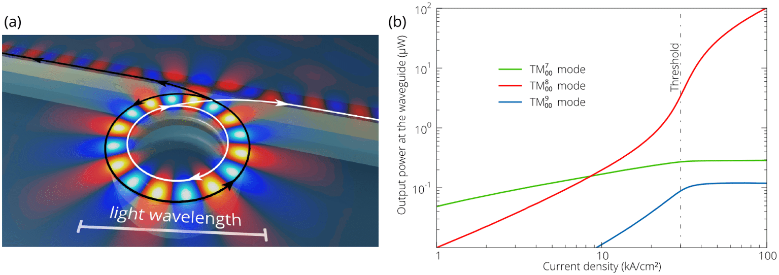
Here, we propose a novel SPP amplification scheme featuring electrical pumping and based on a double-heterostructure tunneling Schottky-barrier Au/InAsP/InGaAs/AlInAs structure for the first time presenting an on-chip subwavelength coherent SPP source based on this approach (Fig. 1). In contrast to most of the nanolasers, our device does not merely emit light into the free-space in a dipole-like fashion, but efficiently couple radiation into in-plane plasmonic (or photonic) waveguides. At room temperature, the threshold current density is only 30 kA/cm2 and is reduced below 0.3 kA/cm2 at cryogenic temperatures. At the same time, the electro-optical conversion efficiency can exceed 30%, which creates the backbone for the next generation of nanophotonic and optoelectronic circuits.

Figure 1. Coherent SPP source coupled to the straight nanoplasmonic waveguide. (b) Input-output characteristic of the SPP source.
dmitry.fedyanin@phystech.edu
Powered by Eventact EMS