")
THIN LAYER BUCKLING IN PEROVSKITE CsPbBr3 NANOBELTS
2The Solid-State Institute, Technion - Israel Institute of Technology, Haifa, Israel
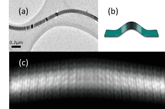
Flexible semiconductor materials, where structural fluctuations and transformations are tolerable and have a low impact on electronic properties, have great potential in future applications. Two-dimensional and thin layer lead halide perovskites are hailed for their unconventional optoelectronic features. In my studies, I discovered a new source of structural deformations via thin layer buckling in colloidal CsPbBr3 nanobelts. The buckled nanobelts` microstructure is determined using transmission electron microscopy (TEM), particularly a selected orientation dark-field imaging (SODFI) technique. With it, we choose two opposite diffracted planes (Bragg point reflections), meaning the two diffracted planes chosen will have opposite orientation, or in other words, opposite angles of scattering. By doing this, we can image different directions of the crystal compared to the electron beam, thus, showing a change in the orientation and its relation to one another. We also used tilting experiments, showing the dependence of the bend contours on the tilt of the sample. When tilting the specimen, we change the diffraction conditions locally, meaning we change the area of the sample which is in the Bragg condition, causing the contrast`s movement. The TEM experiments were done together with image simulations of bent perovskite nanobelts, where the image was generated by a slicing algorithm embedded in the QSTEM simulation package. These simulations showed the effect of the perovskite bend on the phase contrast. To correlate structure properties observed by TEM and topographical buckling of the nanobelts, a correlated cross-analysis of matched TEM-Atomic force microscopy (AFM) scan was used. We had resorted to a finder grid and manual matching of features to narrow down the scans to perform topography measurements of the bend with atomic resolution (in the z-direction), measuring the height variations along the nanobelt. The effect of the bend on the material properties was measured using scanning electron microscopy (SEM)- cathodoluminescence, this measurement showed a significant decrease in local emission from the buckled nanobelt, marking the influence of such mechanical deformations on electronic properties. By employing plate buckling theory to the data, we approximate adhesion forces between the buckled nanobelt and the substrate, marking a limit to sustain such deformation. This work highlights the detrimental effects of mechanical buckling on electronic properties in halide perovskite nanostructures and points towards the capillary action and surface energy. The complete effect of the buckled perovskite crystal lattice on the extent of optoelectronic and other physical properties needs further investigation. However, the forces and the capillary action leading to the buckling in metal-halide perovskites at the nanoscale which is critical, have been identified. These forces should be minimized in fabricating future devices and heterostructures based on nano-perovskites.
The greater vision we take from this work is in the correlation of structural properties extracted from TEM analysis and their contribution to the overall functionality and physical properties emerging from the structure.
(1) Massasa, E. H.; Strassberg, R.; Vurgaft, A.; Kauffmann, Y.; Cohen, N.; Bekenstein, Y. Thin Layer Buckling in Perovskite CsPbBr3Nanobelts. Nano Lett. 2021, 21 (13), 5564–5571.